MX25L12835F
12. ELECTRICAL SPECIFICATIONS
Table 14. ABSOLUTE MAXIMUM RATINGS
RATING
VALUE
Ambient Operating Temperature
Storage Temperature
Applied Input Voltage
Applied Output Voltage
VCC to Ground Potential
Industrial grade
-40°C to 85°C
-65°C to 150°C
-0.5V to VCC+0.5V
-0.5V to VCC+0.5V
-0.5V to VCC+0.5V
NOTICE:
1. Stresses greater than those listed under ABSOLUTE MAXIMUM RATINGS may cause permanent damage
to the device. This is stress rating only and functional operational sections of this specification is not implied.
Exposure to absolute maximum rating conditions for extended period may affect reliability.
2. Specifications contained within the following tables are subject to change.
3. During voltage transitions, all pins may overshoot to VCC+2.0V or -2.0V for period up to 20ns.
4. All input and output pins may overshoot to VCC+0.2V.
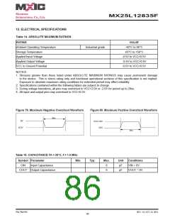
Figure 80. Maximum Positive Overshoot Waveform
Figure 79. Maximum Negative Overshoot Waveform
20ns
0V
VCC+1.0V
-0.5V
2.0V
20ns
Table 15. CAPACITANCE TA = 25°C, f = 1.0 MHz
Symbol Parameter
Min.
Typ.
Max.
Unit
pF
Conditions
VIN = 0V
CIN
Input Capacitance
6
8
COUT Output Capacitance
pF
VOUT = 0V
P/N: PM1795
REV. 1.0, OCT. 23, 2012
86

 Macronix [ MACRONIX INTERNATIONAL ]