MX25L12835F
11. POWER-ON STATE
The device is at below states when power-up:
- Standby mode (please note it is not deep power-down mode)
- Write Enable Latch (WEL) bit is reset
The device must not be selected during power-up and power-down stage unless the VCC achieves below correct
level:
- VCC minimum at power-up stage and then after a delay of tVSL
- GND at power-down
Please note that a pull-up resistor on CS# may ensure a safe and proper power-up/down level.
An internal power-on reset (POR) circuit may protect the device from data corruption and inadvertent data change
during power up state. When VCC is lower than VWI (POR threshold voltage value), the internal logic is reset and
the flash device has no response to any command.
For further protection on the device, if the VCC does not reach the VCC minimum level, the correct operation is not
guaranteed. The read, write, erase, and program command should be sent after the below time delay:
- tVSL after VCC reached VCC minimum level
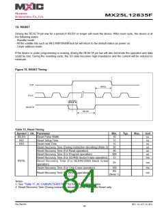
Please refer to the "Figure 85. Power-up Timing".
Note:
- To stabilize the VCC level, the VCC rail decoupled by a suitable capacitor close to package pins is recommend-
ed. (generally around 0.1uF)
- At power-down stage, the VCC drops below VWI level, all operations are disable and device has no response
to any command. The data corruption might occur during the stage while a write, program, erase cycle is in
progress.
P/N: PM1795
REV. 1.0, OCT. 23, 2012
85

 Macronix [ MACRONIX INTERNATIONAL ]