MX25L12835F
13. OPERATING CONDITIONS
At Device Power-Up and Power-Down
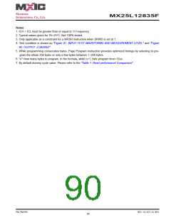
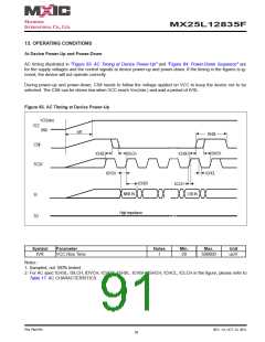
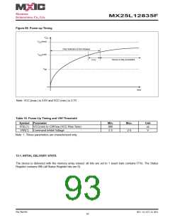
AC timing illustrated in "Figure 83. AC Timing at Device Power-Up" and "Figure 84. Power-Down Sequence" are
for the supply voltages and the control signals at device power-up and power-down. If the timing in the figures is ig-
nored, the device will not operate correctly.
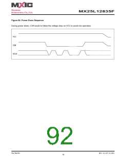
During power-up and power-down, CS# needs to follow the voltage applied on VCC to keep the device not to be
selected. The CS# can be driven low when VCC reach Vcc(min.) and wait a period of tVSL.
Figure 83. AC Timing at Device Power-Up
VCC(min)
VCC
GND
tVR
tSHSL
CS#
tSHCH
tSLCH
tCHSL
tCHSH
SCLK
tDVCH
tCHCL
tCHDX
tCLCH
MSB IN
LSB IN
SI
High Impedance
SO
Symbol
Parameter
Notes
Min.
Max.
Unit
tVR
VCC Rise Time
1
20
500000
us/V
Notes :
1. Sampled, not 100% tested.
2. For AC spec tCHSL, tSLCH, tDVCH, tCHDX, tSHSL, tCHSH, tSHCH, tCHCL, tCLCH in the figure, please refer to
Table 17. AC CHARACTERISTICS.
P/N: PM1795
REV. 1.0, OCT. 23, 2012
91

 Macronix [ MACRONIX INTERNATIONAL ]