MX25L12835F
10. RESET
Driving the RESET# pin low for a period of tRLRH or longer will reset the device. After reset cycle, the device is at
the following states:
- Standby mode
- All the volatile bits such as WEL/WIP/SRAM lock bit will return to the default status as power on.
- 3-byte address mode
If the device is under programming or erasing, driving the RESET# pin low will also terminate the operation and data
could be lost. During the resetting cycle, the SO data becomes high impedance and the current will be reduced to
minimum.
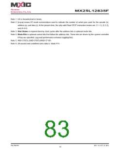
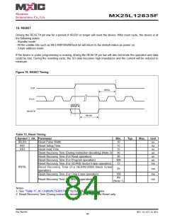
Figure 78. RESET Timing
CS#
tRHSL
SCLK
tRH
tRS
RESET#
tRLRH
Table 13. Reset Timing
Symbol Alt. Parameter
Min.
10
15
Typ.
Max.
Unit
us
ns
tRLRH
tRS
Reset Pulse Width
Reset Setup Time
Reset Hold Time
tRH
15
ns
Reset Recovery Time (During instruction decoding) (Note 2)
Reset Recovery Time (For Read operation)
Reset Recovery Time (For Program operation)
Reset Recovery Time (For SE/4KB Sector Erase operation)
Reset Recovery Time (For BE64K/32KB Block Erase
operation)
30
30
300
12
us
us
us
ms
tRHSL
25
ms
ms
ms
Reset Recovery Time (For Chip Erase operation)
100
tW
(Note 1)
Reset Recovery Time (for WRSR operation)
Notes:
1. See "Table 17. AC CHARACTERISTICS" for tSE/tBE (32KB)/tW data.
2. Reset Recovery Time (During instruction decoding) is for Hardware Reset only.
P/N: PM1795
REV. 1.0, OCT. 23, 2012
84

 Macronix [ MACRONIX INTERNATIONAL ]