MX25L12835F
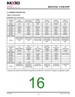
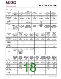
ID/Security Commands
REMS
(read electronic
manufacturer & (QPI ID Read)
device ID)
RDID
RES
ENSO
EXSO
Command
(byte)
QPIID
(read identific- (read electronic
RDSFDP
(enter secured (exit secured
ation)
ID)
OTP)
OTP)
Mode
Address Bytes
SPI
0
SPI/QPI
0
SPI
0
QPI
0
SPI/QPI
3
SPI/QPI
0
SPI/QPI
0
1st byte
2nd byte
3rd byte
4th byte
5th byte
9F (hex)
AB (hex)
90 (hex)
AF (hex)
5A (hex)
B1 (hex)
C1 (hex)
x
x
x
x
ADD1
ADD2
x
ADD1 (Note 1)
ADD3
Dummy (8)
outputs JEDEC to read out
output the
ID in QPI
interface
Read SFDP
mode
to enter the
4K-bit secured 4K-bit secured
OTP mode
to exit the
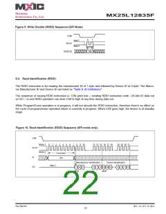
ID: 1-byte
Manufacturer
ID & 2-byte
Device ID
1-byte Device Manufacturer
ID
ID & Device ID
OTP mode
Action
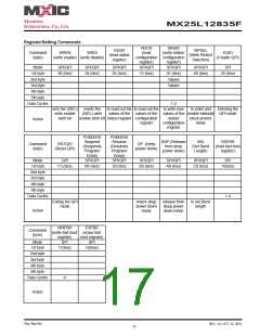
WRSCUR
(write
security
register)
SPI/QPI
WRPASS
(write
password
register)
SPI
RDPASS
(read
password
register)
SPI
RDSCUR
(read security
register)
GBLK
GBULK
WRLR
RDLR
Command
(byte)
(gang block (gang block (write Lock (read Lock
lock)
unlock)
register)
register)
Mode
SPI/QPI
0
SPI/QPI
0
SPI/QPI
0
SPI
0
SPI
0
Address Bytes
0
0
0
1st byte
2nd byte
3rd byte
2B (hex)
2F (hex)
7E (hex)
98 (hex)
2C (hex)
2D (hex)
28 (hex)
27 (hex)
4th byte
5th byte
Data Cycles
2
2
1-8
1-8
to read value to set the
whole chip whole chip
of security lock-down bit write protect unprotect
register
as "1" (once
lock-down,
cannot be
updated)
Action
PASSULK
(password
unlock)
SPI
WRSPB
(SPB bit
program)
SPI
ESSPB
(all SPB bit (read SPB
erase)
SPI
0
RDSPB
SPBLK
(SPB lock
set)
RDSPBLK
(SPB lock
register read) register)
WRDPB
(write DPB
RDDPB
(read DPB
register)
SPI
Command
(byte)
status)
SPI
4
Mode
SPI
SPI
0
SPI
4
Address Bytes
0
4
0
4
1st byte
2nd byte
3rd byte
29 (hex)
E3 (hex)
ADD1
ADD2
ADD3
ADD4
E4 (hex)
E2 (hex)
ADD1
ADD2
ADD3
ADD4
1
A6 (hex)
A7 (hex)
E1 (hex)
ADD1
ADD2
ADD3
ADD4
1
E0 (hex)
ADD1
ADD2
ADD3
ADD4
1
4th byte
5th byte
Data Cycles
8
2
Action
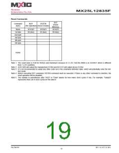
P/N: PM1795
REV. 1.0, OCT. 23, 2012
18

 Macronix [ MACRONIX INTERNATIONAL ]