MX25L12835F
9. COMMAND DESCRIPTION
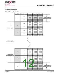
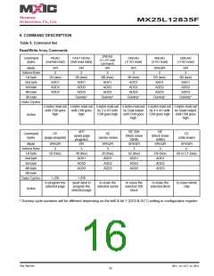
Table 5. Command Set
Read/Write Array Commands
2READ
(2 x I/O read
command)
Command
(byte)
READ
(normal read)
FAST READ
(fast read data)
DREAD
(1I 2O read)
4READ
(4 I/O read)
QREAD
(1I 4O read)
Mode
Address Bytes
1st byte
SPI
3
SPI
3
SPI
3
SPI
3
SPI/QPI
3
SPI
3
03 (hex)
ADD1
ADD2
ADD3
0B (hex)
ADD1
ADD2
ADD3
Dummy*
BB (hex)
ADD1
ADD2
ADD3
Dummy*
3B (hex)
ADD1
ADD2
ADD3
Dummy*
EB (hex)
ADD1
ADD2
ADD3
Dummy*
6B (hex)
ADD1
ADD2
ADD3
Dummy*
2nd byte
3rd byte
4th byte
5th byte
Data Cycles
n bytes read out n bytes read out n bytes read out n bytes read out n bytes read out n bytes read out
until CS# goes
until CS# goes
by 2 x I/O until
CS# goes high
by Dual output
until CS# goes
high
by 4 x I/O until
CS# goes high
by Quad output
until CS# goes
high
high
high
Action
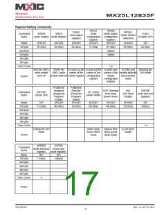
4PP
(quad page
program)
BE 32K
(block erase
32KB)
BE
Command
(byte)
PP
SE
CE
(chip erase)
(block erase
64KB)
(page program)
(sector erase)
Mode
Address Bytes
1st byte
SPI/QPI
3
SPI
3
SPI/QPI
3
SPI/QPI
3
SPI/QPI
3
SPI/QPI
0
02 (hex)
38 (hex)
ADD1
ADD2
ADD3
20 (hex)
ADD1
ADD2
ADD3
52 (hex)
ADD1
ADD2
ADD3
D8 (hex)
ADD1
ADD2
ADD3
60 or C7 (hex)
2nd byte
3rd byte
4th byte
5th byte
1-256
1-256
Data Cycles
to program the
selected page
quad input to
program the
selected page
to erase the
selected sector
to erase the
selected 32K
block
to erase the
selected block
to erase whole
chip
Action
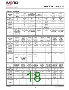
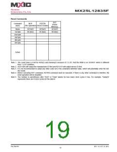
* Dummy cycle numbers will be different depending on the bit6 & bit 7 (DC0 & DC1) setting in configuration register.
P/N: PM1795
REV. 1.0, OCT. 23, 2012
16

 Macronix [ MACRONIX INTERNATIONAL ]