MX25L12835F
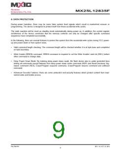
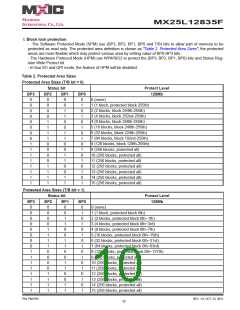
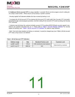
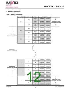
8. DEVICE OPERATION
1. Before a command is issued, status register should be checked to ensure device is ready for the intended op-
eration.
2. When incorrect command is inputted to this device, this device becomes standby mode and keeps the standby
mode until next CS# falling edge. In standby mode, SO pin of this device should be High-Z.
3. When correct command is inputted to this device, this device becomes active mode and keeps the active mode
until next CS# rising edge.
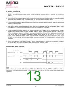
4. Input data is latched on the rising edge of Serial Clock (SCLK) and data shifts out on the falling edge of SCLK.
The difference of Serial mode 0 and mode 3 is shown as "Serial Modes Supported".
5. For the following instructions: RDID, RDSR, RDSCUR, READ, FAST_READ, 2READ, DREAD, 4READ, QREAD,
RDSFDP, RES, REMS, QPIID, RDDPB, RDSPB, RDPASS, RDLR, RDEAR, RDFBR, RDSPBLK, RDCR the
shifted-in instruction sequence is followed by a data-out sequence. After any bit of data being shifted out, the
CS# can be high. For the following instructions: WREN, WRDI, WRSR, SE, BE32K, BE, CE, PP, 4PP, DP,
ENSO, EXSO, WRSCUR, WPSEL, GBLK, GBULK, SPBLK, SUSPEND, RESUME, NOP, RSTEN, RST, EQIO,
RSTQIO the CS# must go high exactly at the byte boundary; otherwise, the instruction will be rejected and not
executed.
6. During the progress of Write Status Register, Program, Erase operation, to access the memory array is neglect-
ed and not affect the current operation of Write Status Register, Program, Erase.
Figure 1. Serial Modes Supported
CPOL CPHA
shift in
shift out
SCLK
SCLK
(Serial mode 0)
(Serial mode 3)
0
1
0
1
SI
MSB
SO
MSB
Note:
CPOL indicates clock polarity of Serial master, CPOL=1 for SCLK high while idle, CPOL=0 for SCLK low while not
transmitting. CPHA indicates clock phase. The combination of CPOL bit and CPHA bit decides which Serial mode is
supported.
P/N: PM1795
REV. 1.0, OCT. 23, 2012
13

 Macronix [ MACRONIX INTERNATIONAL ]