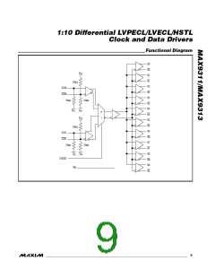
1:10 Differential LVPECL/LVECL/HSTL
Clock and Data Drivers
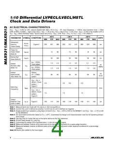
AC ELECTRICAL CHARACTERISTICS
(V
- V = 2.25V to 3.8V, outputs loaded with 50Ω 1ꢀ to V
- 2V, input frequency = 1.5GHz, input transition time = 125ps
CC
CC
EE
(20ꢀ to 80ꢀ), CLKSEL = high or low, V
= V + 1.2V to V , V
= V to V
- 0.15V, V
- V
= 0.15V to the smaller of 3V or
IHD
EE
CC ILD
EE
CC
IHD
ILD
V
CC
- V , unless otherwise noted. Typical values are at V
- V = 3.3V, V
= V -1V, V = V -1.5V.) (Note 7)
CC
IHD
CC ILD CC
EE
EE
-40°C
+25°C
+85°C
PARAMETER SYMBOL CONDITIONS
UNITS
MA
MIN
TYP
MAX
MIN
TYP
MIN
TYP
MAX
Differential
Input-to-
Output Delay
t
t
,
PLHD
Figure 2
220
321
12
380
220
312
410
260
322
400
ps
PHLD
Output-to-
Output Skew
(Note 8)
t
46
12
46
10
35
ps
ps
SKOO
Part-to-Part
Skew (Note 9)
t
30
1.2
1.2
160
2.5
2.6
30
1.2
1.2
190
2.5
2.6
30
1.2
1.2
140
2.5
2.6
SKPP
f
= 1.5GHz,
Clock pattern
IN
Added
Random Jitter
(Note 10)
ps
(RMS)
t
RJ
f
IN
= 3.0GHz,
Clock pattern
Added
Deterministic
Jitter (Note 10)
3Gbps,
223 -1 PRBS
pattern
ps
(p-p)
t
80
95
80
95
80
95
DJ
V
- V
OL
≥
OH
350mV, Clock
pattern,
2.0
2.0
3.0
2.0
Figure 2
Switching
Frequency
f
GHz
MAX
V
- V
OL
≥
OH
500mV, Clock
pattern,
1.5
1.5
1.5
Figure 2
Output
Rise/Fall Time
(20ꢀ to 80ꢀ)
t , t
R
Figure 2
100
112
140
100
116
140
100
121
140
ps
F
Note 1: Measurements are made with the device in thermal equilibrium.
Note 2: Current into a pin is defined as positive. Current out of a pin is defined as negative.
Note 3: Single-ended input operation using V is limited to V
- V = 3.0V to 3.8V for the MAX9311 and V
- V = 2.7V to 3.8V
CC EE
BB
CC
EE
for the MAX9313.
Note 4: DC parameters production tested at T = +25°C. Guaranteed by design and characterization over the full operating temper-
A
ature range.
Note 5: Use V only for inputs that are on the same device as the V reference.
BB
BB
Note 6: All pins open except V
and V
.
CC
EE
Note 7: Guaranteed by design and characterization. Limits are set at 6 sigma.
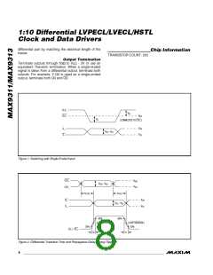
Note 8: Measured between outputs of the same part at the signal crossing points for a same-edge transition.
Note 9: Measured between outputs of different parts at the signal crossing points under identical conditions for a same-edge
transition.
Note 10:Device jitter added to the input signal.
4
_______________________________________________________________________________________

 MAXIM [ MAXIM INTEGRATED PRODUCTS ]