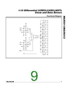
1:10 Differential LVPECL/LVECL/HSTL
Clock and Data Drivers
ABSOLUTE MAXIMUM RATINGS
V
- V ...............................................................................4.1V
Junction-to-Case Thermal Resistance
CC
EE
Inputs (CLK_, CLK_, CLKSEL)..............V - 0.3V to V
+ 0.3V
7mm x 7mm LQFP .....................................................+12°C/W
Operating Temperature Range ...........................-40°C to +85°C
Junction Temperature......................................................+150°C
Storage Temperature Range.............................-ꢁ5°C to +150°C
ESD Protection
EE
CC
CLK_ to CLK_ .................................................................... 3.0V
Continuous Output Current.................................................50mA
Surge Output Current........................................................100mA
V
Sink/Source Current ............................................... 0.ꢁ5mA
BB
Junction-to-Ambient Thermal Resistance in Still Air
7mm x 7mm LQFP .....................................................+90°C/W
Junction-to-Ambient Thermal Resistance with
500 LFPM Airflow
Human Body Model (CLKSEL, CLK_, CLK_,
Q_, Q_, V ).......................................................................2kV
BB
Soldering Temperature (10s)...........................................+300°C
7mm x 7mm LQFP .....................................................+ꢁ0°C/W
Stresses beyond those listed under “Absolute Maximum Ratings” may cause permanent damage to the device. These are stress ratings only, and functional
operation of the device at these or any other conditions beyond those indicated in the operational sections of the specifications is not implied. Exposure to
absolute maximum rating conditions for extended periods may affect device reliability.
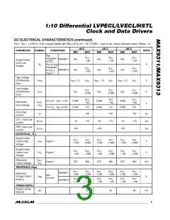
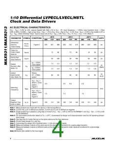
DC ELECTRICAL CHARACTERISTICS
(V - V = +2.25V to +3.8V, outputs loaded with 50Ω 1ꢀ to V - 2V, CLKSEL = high or low, unless otherwise noted.) (Notes 1–4)
CC
EE
CC
-40°C
+25°C
+85°C
PARAMETER
SYMBOL
CONDITIONS
UNITS
MIN
MAX
MIN
MAX
MIN
MAX
SINGLE-ENDED INPUT (CLKSEL)
V
V
V
CC
- 1.23
CC
CC
MAX9311
MAX9313
MAX9311
MAX9313
V
V
V
CC
CC
CC
Internal
- 1.23
- 1.23
Input High
Voltage
V
V
V
V
IH
BB
V
V
V
CC
- 1.165
CC
CC
threshold
V
V
V
V
V
V
CC
CC
CC
CC
CC
CC
- 1.165
- 1.165
V
V
V
V
V
V
EE
EE
EE
EE
EE
EE
Internal
- 1.62
- 1.62
- 1.62
Input Low
Voltage
V
V
BB
IL
V
V
V
CC
- 1.475
CC
CC
threshold
- 1.475
- 1.475
Input High
Current
I
150
150
150
µA
µA
IH
Input Low
Current
I
-10
+10
-10
+10
-10
+10
IL
DIFFERENTIAL INPUTS (CLK_, CLK_)
V
BB
V
V
V
CC
- 1.23
CC
CC
connected
to CLK_
(V for V
connected
to CLK_),
Figure 1
MAX9311
MAX9313
V
V
V
V
V
V
CC
CC
CC
CC
CC
CC
Single-Ended
Input High
Voltage
- 1.23
- 1.23
V
V
IH
IL
BB
V
V
V
CC
- 1.165
CC
CC
- 1.165
- 1.165
2
_______________________________________________________________________________________

 MAXIM [ MAXIM INTEGRATED PRODUCTS ]