1:10 Differential LVPECL/LVECL/HSTL
Clock and Data Drivers
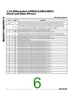
When using the V
reference output, bypass it with a
BB
Detailed Description
0.01µF ceramic capacitor to V . If the V reference is
CC
BB
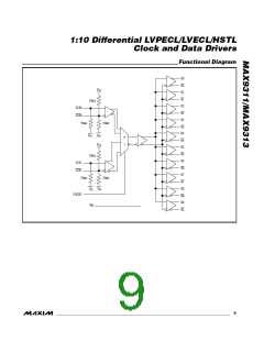
The MAX9311/MAX9313 are low skew, 1-to-10 differen-
tial drivers designed for clock and data distribution.
not used, it can be left open. The V
source or sink 0.5mA, which is sufficient to drive two
reference can
BB
A 2:1 mux selects between the two differential inputs,
CLK0, CLK0 and CLK1, CLK1. The 2:1 mux is switched
by the single-ended CLKSEL input. A logic low selects
the CLK0, CLK0 input. A logic high selects the CLK1,
CLK1 input. The logic threshold for CLKSEL is set by an
inputs. Use V
only for inputs that are on the same
BB
device as the V reference.
BB
The maximum magnitude of the differential input from
CLK_ to CLK_ is 3.0V or V
This limit also applies to the difference between any ref-
erence voltage input and a single-ended input.
- V , whichever is less.
EE
CC
internal V
voltage reference. The CLKSEL input can
BB
be driven to V
and V or by a single-ended LVPECL/
EE
CC
The differential inputs have bias resistors that drive the
outputs to a differential low when the inputs are open.
The inverting inputs (CLK0 and CLK1) are biased with a
LVECL signal. The selected input is reproduced at 10
differential outputs.
For interfacing to differential HSTL and LVPECL signals,
these devices operate over a +2.25V to +3.8V supply
range, allowing high-performance clock or data distribu-
tion in systems with a nominal +2.5V or +3.3V supply.
For differential LVECL operation, these devices operate
from a -2.25V to -3.8V supply.
75kΩ pullup to V
and a 75kΩ pulldown to V . The
EE
CC
noninverting inputs (CLK0 and CLK1) are biased with a
75kΩ pulldown to V . The single-ended CLKSEL input
EE
does not have a bias resistor. If not driven, pull CLKSEL
up or down with a 1kHz resistor (see Pin Description).
Specifications for the high and low voltages of a differen-
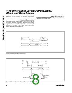
The differential inputs can be configured to accept sin-
tial input (V
and V ) and the differential input volt-
ILD
ILD
IHD
IHD
gle-ended inputs when operating at approximately V
-
CC
age (V
- V ) apply simultaneously (V
cannot be
IHD
ILD
V
EE
= +3.0V to +3.8V for the MAX9311 or V
- V
=
CC
EE
higher than V ).
+2.7V to +3.8V for the MAX9313. This is accomplished
Output levels are referenced to V
LVPECL or LVECL, depending on the level of the V
and are considered
CC
by connecting the on-chip reference voltage, V , to an
BB
CC
input as a reference. For example, the differential CLK0,
supply. With V
EE
outputs are LVECL when V
connected to a positive supply and
CC
CLK0 input is converted to a noninverting, single-ended
V
connected to GND, the outputs are LVPECL. The
input by connecting V
to CLK0 and connecting the
BB
is connected to GND and
CC
single-ended input to CLK0. Similarly, an inverting input
V
EE
is connected to a negative supply.
is obtained by connecting V to CLK0 and connecting
BB
the single-ended input to CLK0. With a differential input
A single-ended input of at least V
95mV or a differen-
BB
configured as single-ended (using V ), the single-
BB
tial input of at least 95mV switches the outputs to the
and V levels specified in the DC Electrical
ended input can be driven to V
and V or with a sin-
CC
EE
V
OH
OL
gle-ended LVPECL/LVECL signal.
When a differential input is configured as a single-ended
input (using V ), the approximate supply range is V
Characteristics table.
Applications Information
-
CC
EE
BB
V
EE
= +3.0V to +3.8V for the MAX9311 and V
- V
=
CC
Supply Bypassing
to V with high-frequency surface-mount
+2.7V to +3.8V for the MAX9313. This is because one of
the inputs must be V + 1.2V or higher for proper oper-
Bypass V
CC
EE
EE
ceramic 0.1µF and 0.01µF capacitors in parallel as close
to the device as possible, with the 0.01µF value capaci-
tor closest to the device. Use multiple parallel vias for
ation of the input stage. V must be at least V + 1.2V
BB
EE
because it becomes the high-level input when the other
(single-ended) input swings below it. Therefore, mini-
low inductance. When using the V
reference output,
BB
mum V = V + 1.2V.
BB
EE
bypass it with a 0.01µF ceramic capacitor to V
(if the
CC
V
BB
reference is not used, it can be left open).
The minimum V
output for the MAX9311 is V
-
CC
BB
1.525V and the minimum V output for the MAX9313 is
BB
Traces
V
- 1.38V. Substituting the minimum V
output for
CC
BB
Input and output trace characteristics affect the perfor-
mance of the MAX9311/MAX9313. Connect each signal
of a differential input or output to a 50Ω characteristic
impedance trace. Minimize the number of vias to prevent
impedance discontinuities. Reduce reflections by main-
taining the 50Ω characteristic impedance through con-
nectors and across cables. Reduce skew within a
each device into V = V + 1.2V results in a minimum
BB
EE
supply of 2.725V for the MAX9311 and 2.58V for the
MAX9313. Rounding up to standard supplies gives the
single-ended operating supply ranges of V
- V
=
CC
EE
3.0V to 3.8V for the MAX9311 and V
3.8V for the MAX9313.
- V = 2.7V to
CC
EE
_______________________________________________________________________________________
7

 MAXIM [ MAXIM INTEGRATED PRODUCTS ]