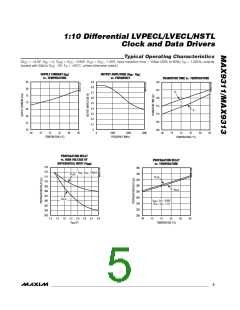
19-2078; Rev 2; 10/02
1:10 Differential LVPECL/LVECL/HSTL
Clock and Data Drivers
General Description
Features
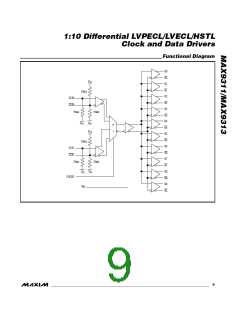
The MAX9311/MAX9313 are low-skew, 1-to-10 differen-
tial drivers designed for clock and data distribution.
These devices allow selection between two inputs. The
selected input is reproduced at 10 differential outputs.
The differential inputs can be adapted to accept single-
ꢀ +2.25V to +3.8V Differential HSTL/LVPECL
Operation
ꢀ -2.25V to -3.8V LVECL Operation
ꢀ 30ps (typ) Part-to-Part Skew
ꢀ 12ps (typ) Output-to-Output Skew
ꢀ 312ps (typ) Propagation Delay
ꢀ ≥ 300mV Differential Output at 3GHz
ꢀ On-Chip Reference for Single-Ended Inputs
ꢀ Output Low with Open Input
ended inputs by connecting the on-chip V
one input as a reference voltage.
supply to
BB
The MAX9311/MAX9313 feature low part-to-part skew
(30ps) and output-to-output skew (12ps), making them
ideal for clock and data distribution across a backplane
or a board. For interfacing to differential HSTL and
LVPECL signals, these devices operate over a +2.25V
to +3.8V supply range, allowing high-performance clock
or data distribution in systems with a nominal +2.5V or
+3.3V supply. For differential LVECL operation, these
devices operate from a -2.25V to -3.8V supply.
ꢀ Pin Compatible with MC100LVEP111 (MAX9311)
and MC100EP111 (MAX9313)
ꢀ Offered in Tiny QFN* Package (70% Smaller
The MAX9311 features an on-chip V reference output
BB
of 1.425V below the positive supply voltage. The
Footprint than LQFP)
MAX9313 offers an on-chip V
reference output of
BB
Ordering Information
1.32V below the positive supply voltage.
PART
TEMP. RANGE
PIN-PACKAGE
Both devices are offered in space-saving, 32-pin 5mm ✕
5mm TQFP, 5mm x 5mm QFN, and industry-standard
32-pin 7mm x 7mm LQFP packages.
MAX9311ECJ
-40°C to +85°C
32 LQFP (7mm ✕ 7mm)
32 QFN (5mm ✕ 5mm)
32 TQFP (5mm ✕ 5mm)
32 LQFP (7mm ✕ 7mm)
32 QFN (5mm ✕ 5mm)
32 TQFP (5mm ✕ 5mm)
MAX9311EGJ* -40°C to +85°C
MAX9311EHJ*
MAX9313ECJ
MAX9313EGJ*
MAX9313EHJ*
-40°C to +85°C
-40°C to +85°C
-40°C to +85°C
-40°C to +85°C
Applications
Precision Clock Distribution
Low-Jitter Data Repeater
*Future product—contact factory for availability.
Pin Configuration
TOP VIEW
V
Q0 Q0 Q1 Q1 Q2 Q2
V
CC
CC
32 31 30 29 28 27 26 25
V
1
2
3
4
5
6
7
8
24 Q3
Q3
CC
×
×
CLKSEL
CLK0
23
LQFP (7mm 7mm), TQFP (5mm 5mm),
QFN (NO LEADS EXTENDING FROM QFN PACKAGE)
22 Q4
21 Q4
20 Q5
19 Q5
18 Q6
17 Q6
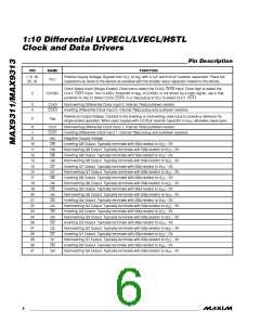
MAX9311/MAX9313
CLK0
MAX9311
MAX9313
CLKSEL CLK0, CLK0 CLK1, CLK1
V
BB
0
1
ON
OFF
ON
CLK1
CLK1
OFF
V
EE
9
10 11 12 13 14 15 16
Q9 Q9 Q8 Q8 Q7 Q7
V
V
CC
CC
________________________________________________________________ Maxim Integrated Products
1
For pricing, delivery, and ordering information, please contact Maxim/Dallas Direct! at
1-888-629-4642, or visit Maxim’s website at www.maxim-ic.com.

 MAXIM [ MAXIM INTEGRATED PRODUCTS ]