1:10 Differential LVPECL/LVECL/HSTL
Clock and Data Drivers
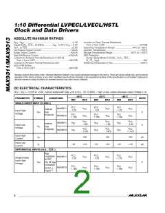
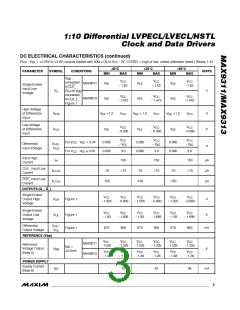
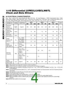
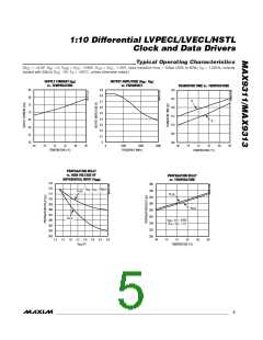
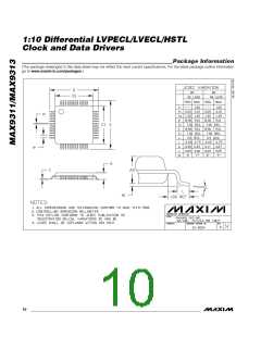
Pin Description
PIN
NAME
FUNCTION
1, 9, 16,
25, 32
Positive Supply Voltage. Bypass from V
CC
capacitors as close to the device as possible with the smaller value capacitor closest to the device.
to V with 0.1µF and 0.01µF ceramic capacitors. Place the
EE
V
CC
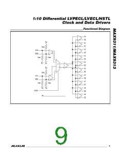
Clock Select Input (Single-Ended). Drive low to select the CLK0, CLK0 input. Drive high to select the
2
CLKSEL CLK1, CLK1 input. The CLKSEL threshold is V . If CLKSEL is not driven by a logic signal, use a 1kΩ
BB
pulldown to V to select CLK0, CLK0, or a 1kΩ pullup to V to select CLK1, CLK1.
EE
CC
3
4
CLK0
Noninverting Differential Clock Input 0. Internal 75kΩ pulldown resistor.
CLK0
Inverting Differential Clock Input 0. Internal 75kΩ pullup and pulldown resistors.
Reference Output Voltage. Connect to the inverting or noninverting clock input to provide a reference for
single-ended operation. When used, bypass with a 0.01µF ceramic capacitor to V ; otherwise, leave open.
CC
5
V
BB
6
CLK1
Noninverting Differential Clock Input 1. Internal 75kΩ pulldown resistor.
Inverting Differential Clock Input 1. Internal 75kΩ pullup and pulldown resistors.
Negative Supply Voltage
7
CLK1
8
V
EE
10
11
12
13
14
15
17
18
19
20
21
22
23
24
26
27
28
29
30
31
Q9
Q9
Q8
Q8
Q7
Q7
Q6
Q6
Q5
Q5
Q4
Q4
Q3
Q3
Q2
Q2
Q1
Q1
Q0
Q0
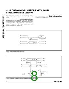
Inverting Q9 Output. Typically terminate with 50Ω resistor to V
- 2V.
CC
Noninverting Q9 Output. Typically terminate with 50Ω resistor to V - 2V.
CC
Inverting Q8 Output. Typically terminate with 50Ω resistor to V
- 2V.
CC
Noninverting Q8 Output. Typically terminate with 50Ω resistor to V - 2V.
CC
Inverting Q7 Output. Typically terminate with 50Ω resistor to V
- 2V.
CC
Noninverting Q7 Output. Typically terminate with 50Ω resistor to V - 2V.
CC
Inverting Q6 Output. Typically terminate with 50Ω resistor to V
- 2V.
CC
Noninverting Q6 Output. Typically terminate with 50Ω resistor to V - 2V.
CC
Inverting Q5 Output. Typically terminate with 50Ω resistor to V
- 2V.
CC
Noninverting Q5 Output. Typically terminate with 50Ω resistor to V - 2V.
CC
Inverting Q4 Output. Typically terminate with 50Ω resistor to V
- 2V.
CC
Noninverting Q4 Output. Typically terminate with 50Ω resistor to V - 2V.
CC
Inverting Q3 Output. Typically terminate with 50Ω resistor to V
- 2V.
CC
Noninverting Q3 Output. Typically terminate with 50Ω resistor to V - 2V.
CC
Inverting Q2 Output. Typically terminate with 50Ω resistor to V
- 2V.
CC
Noninverting Q2 Output. Typically terminate with 50Ω resistor to V - 2V.
CC
Inverting Q1 Output. Typically terminate with 50Ω resistor to V
- 2V.
CC
Noninverting Q1 Output. Typically terminate with 50Ω resistor to V - 2V.
CC
Inverting Q0 Output. Typically terminate with 50Ω resistor to V
- 2V.
CC
Noninverting Q0 Output. Typically terminate with 50Ω resistor to V - 2V.
CC
6
_______________________________________________________________________________________

 MAXIM [ MAXIM INTEGRATED PRODUCTS ]