3 .0 V/3 .3 V Ad ju s t a b le Mic ro p ro c e s s o r
S u p e rvis o ry Circ u it s
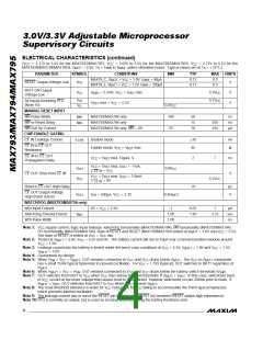
ELECTRICAL CHARACTERISTICS (continued)
(V
= 3.17V to 5.5V for the MAX793T/MAX795T, V
= 3.02V to 5.5V for the MAX793S/MAX795S, V
= 2.72V to 5.5V for the
CC
CC
CC
MAX793R/MAX794/MAX795R, V
= 3.6V, T = T
to T , unless otherwise noted. Typical values are at T = +25°C.)
MAX A
BATT
A
MIN
PARAMETER
SYMBOL
CONDITIONS
= V = 1.0V, I = 40µA
SINK
MIN
TYP
0.13
0.17
MAX
0.3
UNITS
MAX79_C, V
BATT
CC
RESET Output Voltage Low
V
OL
V
MAX79_E, V
= V = 1.2V, I = 200µA
SINK
0.3
BATT
CC
BATT ON Output
Voltage Low
V
I
= 3.2mA, V = V
max
0.2V
CC
V
V
OL
SINK
CC
RST
V
0.7V
CC
All Inputs Including PFO
(Note 10)
IH
V
max < V < 5.5V
CC
RST
V
0.3V
CC
IL
MANUAL RESET INPUT
MR Pulse Width
t
MAX793/MAX794 only
MAX793/MAX794 only
100
25
50
75
70
ns
ns
MR
MR-to-Reset Delay
t
250
250
MD
MR Pull-Up Current
CHIP-ENABLE GATING
CE IN Leakage Current
MAX793/MAX794 only, MR = 0V
µA
I
Disable mode
±10
46
nA
LEAK
CE IN-to-CE OUT
Resistance
Enable mode, V = V
max
Ω
CC
RST
CE IN-to-CE OUT
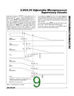
Propagation Delay
V
= V
max, Figure 9
2
7
ns
V
CC
RST
V
= V
max, I
= -1mA,
CC
RST
OUT
V
0.8V
CC
OH
V
= V
CC
34/MAX795
CE IN
CE OUT Drive from CE IN
Reset to CE OUT High Delay
V
= V
max, I
= 1.6mA,
CC
RST
OUT
V
OL
0.2V
CC
V
= 0V
CE IN
10
µs
V
CE OUT Output Voltage
High (reset active)
V
OH
I
OH
= 500µA, V < 2.3V
0.8V
BATT
CC
WATCHDOG (MAX793/MAX794 only)
WDI Input Current
0V < V < 5.5V
-1
0.01
1.60
1
µA
sec
ns
CC
Watchdog Timeout Period
WDI Pulse Width
t
1.00
1.00
2.25
WD
Note 1:
V
supply current, logic input leakage, watchdog functionality (MAX793/MAX794), MR functionality (MAX793/MAX794),
CC
PFI functionality (MAX793/MAX794), state of RESET and RESET (MAX793/MAX794) tested at V
= 3.6V and V = 5.5V.
CC
BATT
The state of RESET is tested at V = V min.
CC
CC
Note 2: Tested at V
= 3.6V, V = 3.5V and 0V. The battery current will rise to 10µA over a narrow transition window around
BATT
CC
V
CC
= 1.9V.
Note 3: Leakage current into the battery is tested under the worst-case conditions at V = 5.5V, V
= 1.8V and V = 1.5V,
CC
CC
BATT
V
BATT
= 1.0V.
Note 4: Guaranteed by design.
Note 5: When V > V > V
, OUT remains connected to V until V drops below V
. The V -to-V
comparator
SW
CC
BATT
CC
CC
BATT
CC
BATT
has a small 15mV typical hysteresis to prevent oscillation. For V < 1.75V (typical), OUT switches to BATT regardless of
CC
V
.
BATT
Note 6: When V
> V > V , OUT remains connected to V until V drops below the battery switch threshold (V ).
CC SW CC CC SW
BATT
Note 7: OUT switches from BATT to V when V rises above the reset threshold, if V
> V . In this case, switchover back
CC
CC
BATT
RST
to V occurs at the exact voltage that causes reset to be asserted, however switchover occurs 200ms prior to reset. If
CC
V
BATT
< V , OUT switches from BATT to V when V exceeds V
.
RST
CC
CC
BATT
Note 8: The reset threshold tolerance is wider for V rising than for V falling to accommodate the 10mV typical hysteresis,
CC
CC
which prevents internal oscillation.
Note 9: The leakage current into or out of the RESET pin is tested with RESET not asserted (RESET output high impedance).
Note 10: PFO is normally an output, but is used as an input when activating the battery freshness seal.
4
_______________________________________________________________________________________

 MAXIM [ MAXIM INTEGRATED PRODUCTS ]