Trip le -Ou t p u t P o w e r-S u p p ly
Co n t ro lle r fo r No t e b o o k Co m p u t e rs
MAX782
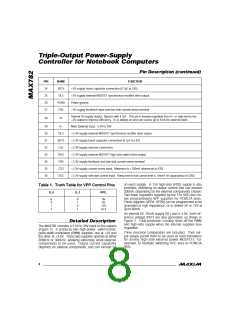
BATTERY INPUT
5.5V TO 30V
(NOTE 1)
C13
33µF
C1
33µF
29
28
VL
+5V at 5mA
C2
4.7µF
V+
DA0
16
15
18
17
9
VPPA
VPPB
VDD
C11
1µF
0V, 5V, 12V
0V, 5V, 12V
D2
VPP
CONTROL
INPUTS
DA1
11
10
DB0
DB1
C10
1µF
+15V AT 300mA, SEE
HIGH-SIDE SUPPLY (VDD)
SECTION.
D1A
1N4148
D1B
1N4148
EC11FS1
MAX782
C4
C5
31
33
32
24
22
23
25
21
0.1µF
C12
BST3
DH3
BST5
DH5
LX5
2.2µF
0.1µF
1:2.2
N2
N1
R1
25mΩ
L1
10µH
+3.3V at 3A
+5V at 3A
C6
LX3
DL3
L2 10µH
D4
1N5819
30
35
R2
20mΩ
D3
DL5
N4
1N5819
N3
C14 C7
150µF150µF
330µF
CS3
FB3
CS5
FB5
34
36
1
27
(NOTE 2)
(NOTE 2)
20
C8
C9
0.01µF
SS3
SS5
VH
0.01µF
5
+3.3V ON/OFF
+5V ON/OFF
OSC SYNC
COMPARATOR SUPPLY INPUT
COMPARATOR INPUTS
ON3
ON5
SYNC
2, 3, 4
19
14
3
3
D1-D3
Q1-Q3
8, 7, 6
COMPARATOR OUTPUTS
GND REF PGND
12 13 26
N1-N4 = Si9410DY
NOTE 1: BATTERY VOLTAGE RANGE 6.5V to 30V
3.3V AT 5mA
WITH COMPONENTS SHOWN
SEE LOW-VOLTAGE (6-CELL) OPERATION SECTION.
NOTE 2: SEE FIGURE 5.
C3
1µF
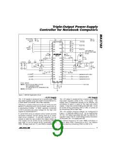
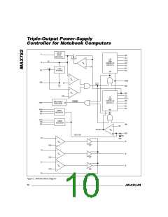
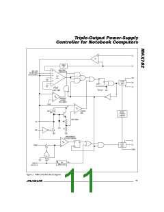
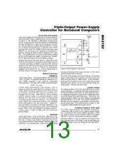
Figure 1. MAX782 Application Circuit
+3 .3 V S u p p ly
+5 V S u p p ly
The +3.3V supply is produced by a current-mode PWM
step-down regulator using two small N-channel MOSFETs,
a catch diode, an inductor, and a filter capacitor.
The +5V output is produced by a current-mode PWM
step-down regulator similar to the +3.3V supply. This
supply uses a transformer primary as its inductor, the
secondary of which is used for the high-side (VDD)
supply. It also has current limiting and soft-start. It can
be turned off by connecting ON5 to GND, or turned on
by connecting ON5 to logic high.
Efficiency is greatly enhanced by the use of the second
MOSFET (connected from LX3 to PGND), which acts as
a synchronous rectifier. A 100nF capacitor connected
to BST3 provides the drive voltage for the high-side
(upper) N-channel MOSFET.
The +5V supply’s dropout voltage, as configured in
Figure 1, is typically 400mV at 2A. As V approaches
IN
A current limit set by an external sense resistor prevents
excessive inductor current during start-up or under
short-circuit conditions. A soft-start capacitor can be
chosen to tailor the rate at which the output ramps up.
This supply can be turned on by connecting ON3 to
logic high, or can be turned off by connecting ON3 to
GND. All logic levels are TTL and CMOS compatible.
5V, the +5V output gracefully falls with V until the VL
IN
regulator output hits its undervoltage lockout threshold.
At this point, the +5V supply turns off.
The d e fa ult fre q ue nc y for b oth PWM c ontrolle rs is
300kHz (with SYNC connected to REF), but 200kHz
may be used by connecting SYNC to GND or VL.
_______________________________________________________________________________________
9

 MAXIM [ MAXIM INTEGRATED PRODUCTS ]