Trip le -Ou t p u t P o w e r-S u p p ly
Co n t ro lle r fo r No t e b o o k Co m p u t e rs
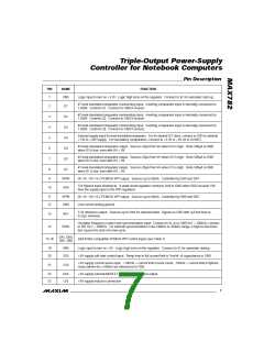
_________________________________________________P in De s c rip t io n (c o n t in u e d )
PIN
24
NAME
BST5
DL5
FUNCTION
+5V-supply boost capacitor connection (0.1µF to LX5)
25
+5V-supply external MOSFET synchronous-rectifier drive output
Power ground
MAX782
26
PGND
FB5
27
+5V-supply feedback input and low-side current-sense terminal
Internal 5V-supply output. Bypass with 4.7µF. This pin is linearly regulated from V+ or switched to the
+5V output to improve efficiency. VL is always on and can source up to 5mA for external loads.
28
VL
29
30
31
32
33
34
35
36
V+
DL3
BST3
LX3
Main (battery) input: 5.5V to 30V
+3.3V-supply external MOSFET synchronous-rectifier drive output
+3.3V-supply boost capacitor connection (0.1µF to LX3)
+3.3V-supply inductor connection
DH3
FB3
CS3
SS3
+3.3V-supply external MOSFET high-side switch-drive output
+3.3V-supply feedback and low-side current-sense terminal
+3.3V-supply current-sense input. Maximum is +100mV referenced to FB3.
+3.3V-supply soft-start control input. Ramp time to full current limit is 1ms/nF of capacitance to GND.
on each supply. A 15V high-side (VDD) supply is also
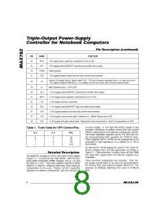
Table 1. Truth Table for VPP Control Pins
provided, delivering an output current that can exceed
300mA, depending on the external components chosen.
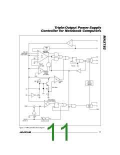
Two linear regulators supplied by the 15V VDD line cre-
ate programmable VPP supplies for PCMCIA slots.
These supplies (VPPA, VPPB) can be programmed to be
grounded or high impedance, or to deliver 5V or 12V at
up to 60mA.
D_0
D_1
VPP_
0
0
1
1
0
1
0
1
0V
5V
12V
Hi-Z
An internal 5V, 25mA supply (VL) and a 3.3V, 5mA ref-
erence voltage (REF) are also generated, as shown in
Figure 2. Fault-protection circuitry shuts off the PWM
and high-side supply when the internal supplies lose
regulation.
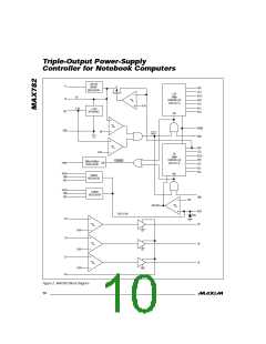
_______________De t a ile d De s c rip t io n
The MAX782 converts a 5.5V to 30V input to five outputs
(Figure 1). It produces two high-power, switch-mode,
pulse-width modulated (PWM) supplies, one at +5V and
the other at +3.3V. These two supplies operate at either
200kHz or 300kHz, allowing extremely small external
components to be used. Output current capability
depends on external components, and can exceed 5A
Three precision comparators are included. Their out-
put stages permit them to be used as level translators
for driving high-side external power MOSFETs: For
example, to facilitate switching VCC lines to PCMCIA
slots.
8
_______________________________________________________________________________________

 MAXIM [ MAXIM INTEGRATED PRODUCTS ]