±±5ꢀk EꢁDꢂ-rotected, HighꢂDrive Current, Dualꢂ/Quadꢂ/
OctalꢂLevel Translators with ꢁpeedꢂUp Circuitry
t
t
RVCC
FVCC
V
V
CC
L
90%
90%
V
EN
V
CC
L
MAX3394E
MAX3395E
MAX3396E
I/O V
L
50%
50%
V
V
L
CC
50%
50%
I/O V
L_
I/O V
CC_
10%
I/O V
10%
CC
50Ω
C
IOVCC
t
I/OVL-VCC
t
I/OVL-VCC
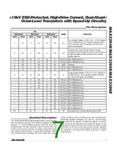
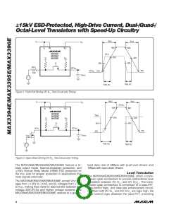
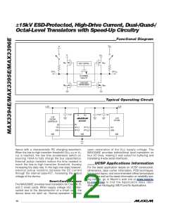
Figure 1. Push-Pull Sriving I/O V Test Circuit and Timing
L_
t
t
RVCC
FVCC
V
L
V
CC
I/O V
CC
90%
90%
EN
V
V
L
CC
MAX3394E
MAX3395E
MAX3396E
V
GATE
50%
50%
V
V
L
CC
50%
50%
I/O V
I/O V
CC_
L_
10%
10%
45/MAX396E
C
IOVCC
V
GATE
t
I/OVL-VCC
t
I/OVL-VCC
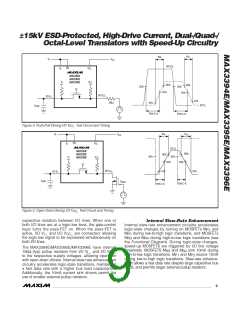
Figure 2. Open-Srain Sriving I/O V Test Circuit and Timing
L_
The MAX3394E/MAX3395E/MAX3396E feature a tri-
state output mode, thermal-shutdown protection, and
15kV ꢀuman ꢁody Model ꢂꢀꢁMꢃ EꢄS protection on
teed data rate of 6Mbps with push-pull drivers and
1Mbps with open-drain drivers.
Level Translation
The MAX3394E/MAX3395E/MAX3396E utilize a trans-
mission gate architecture to provide bidirectional level
the V
side for greater protection in applications that
CC
route signals externally.
The MAX3394E/MAX3395E/MAX3396E accept V
volt-
CC
translation between I/O V _ and I/O V _. The trans-
L
CC
ages from +1.65V to +5.5V, and V voltages from +1.2V
L
mission gate architecture is comprised of a pass-FET,
gate-control logic, and slew-rate enhancement circuit-
to V , making them ideal for data transfer between low-
CC
voltage AꢄIC/PLSs and higher voltage systems. The
MAX3394E/MAX3395E/MAX3396E operate at a guaran-
ry. When both I/O V _ and I/O V _ are logic high, the
L
CC
gate-control logic disables the pass-FET, providing
8
_______________________________________________________________________________________

 MAXIM [ MAXIM INTEGRATED PRODUCTS ]