±±5ꢀk EꢁDꢂ-rotected, HighꢂDrive Current, Dualꢂ/Quadꢂ/
OctalꢂLevel Translators with ꢁpeedꢂUp Circuitry
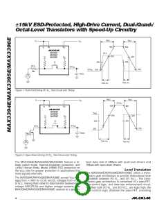
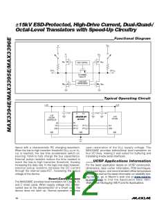
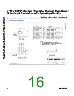
Functional Diagram
V
CC
V
L
V
L
V
CC
M
P1
M
P2
GATE CONTROL
I/O V
I/O V
L_
CC_
N-CHANNEL
PASS-FET
SLEW-RATE
ENHANCEMENT
M
N3
M
N4
Typical Operating Circuit
+1.8V
+3.3V
0.1μF
1μF
0.1μF
V
V
L
CC
+1.8V
SYSTEM
CONTROLLER
+3.3V
SYSTEM
MAX3394E
EN
EN
I/O V
I/O V
1
I/O V 1
L
CLK
CLK
CC
I/O V 2
L
2
DATA
DATA
CC
45/MAX396E
GND
GND
GND
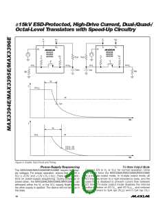
itance with a characteristic RC charging waveform.
When the low-to-high transition threshold ꢂV or V
upon restoration of the V
supply voltage. The
CC
MAX3395E provides bidirectional level translation on
four I/O lines, making it well suited for buffering and
translating 4-wire serial interfaces.
CC-Tꢀ
L-
ꢃ is reached, the rise time accelerators switch on,
Tꢀ
sourcing 15mA to fully charge the bus capacitance.
External pullup resistors reduce the time needed to
reach the low-to-high transition threshold, thereby
increasing the data rate. In the logic-low state however,
external pullup resistors increase the SC current
through the internal pass-FET, increasing the output
voltage of the device.
UCꢁ- Applications Information
For the latest application details on UCꢄP construction,
dimensions, tape carrier information, PCꢁ techniques,
bump-pad layout, and recommended reflow temperature
profiles, as well as the latest information on reliability test-
ing results, go to Maxim’s web site at www.maxim-
ic.com/ucsp to find the Application Note 1891:
Wafer-Level Packaging ꢂWLPꢃ and Its Applications.
ꢁmartꢂCard Interface
The MAX3395E provides level translation for Class A, ꢁ,
and C smart cards. When supply voltage V
is inter-
CC
rupted due to the disconnection of a smart card, the
device does not latch up. Normal operation resumes
12 ______________________________________________________________________________________

 MAXIM [ MAXIM INTEGRATED PRODUCTS ]