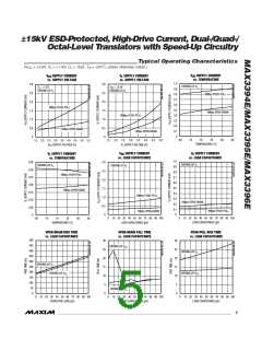
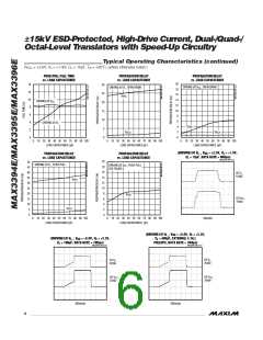
±±5ꢀk EꢁDꢂ-rotected, HighꢂDrive Current, Dualꢂ/Quadꢂ/
OctalꢂLevel Translators with ꢁpeedꢂUp Circuitry
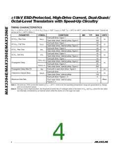
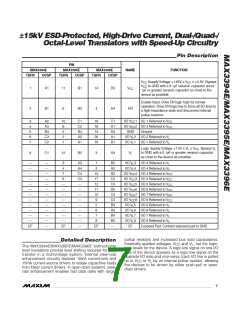
TIMING CHARACTERISTICS
ꢂV
CC
= +1.65V to +5.5V, V = +1.2V to V ; C
≤ 15pF, C ≤ 15pF; T = -40°C to +85°C, unless otherwise noted. Typical val-
IOVCC A
L
CC IOVL
ues are at T = +25°C.ꢃ ꢂNote 1ꢃ
A
PARAMETER
SYMBOL
CONDITIONS
MIN
TYP
MAX
50
UNITS
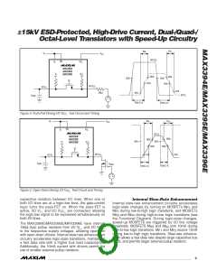
Push-pull driver, Figure 1
I/O V _ Rise Time
t
ns
CC
RVCC
Open-drain driver, internal pullup, Figure 2
Push-pull driver, Figure 1
500
50
I/O V _ Fall Time
t
ns
ns
ns
CC
FVCC
Open-drain driver, internal pullup, Figure 2
Push-pull driver, Figure 3
50
50
I/O V _ Rise Time
t
RVL
L
Open-drain driver, internal pullup, Figure 4
Push-pull driver, Figure 3
500
50
I/O V _ Fall Time
L
t
FVL
Open-drain driver, internal pullup, Figure 4
Push-pull driver, Figure 1
50
50
t
t
I/OVL-VCC
I/OVCC-VL
Open-drain driver, internal pullup, Figure 2
Push-pull driver, Figure 3
600
50
Propagation Selay
ns
Open-drain driver, internal pullup, Figure 4
Push-pull or open-drain driver, Figure 5
Push-pull driver
600
5
Propagation Selay After EN
Channel-to-Channel ꢄkew
t
µs
ns
EN
5
t
ꢄKEW
Open-drain driver, internal pullup
Push-pull driver, Figures 1, 3
100
6
Maximum Sata Rate
Mbps
Open-drain driver, internal pullup,
Figures 2, 4
1
Note 1: All units are 100% production tested at T = +25°C. Limits over the operating temperature range are guaranteed by design
A
and not production tested.
Note 2: Suring a low-to-high transition, the threshold at which the I/O changes state is the lower of V and V
since the two sides
ILC
ILL
are internally connected by an internal switch while the device is in the logic-low state.
45/MAX396E
4
_______________________________________________________________________________________

 MAXIM [ MAXIM INTEGRATED PRODUCTS ]