±±5ꢀk EꢁDꢂ-rotected, HighꢂDrive Current, Dualꢂ/Quadꢂ/
OctalꢂLevel Translators with ꢁpeedꢂUp Circuitry
45/MAX396E
R
C
R
D
1MΩ
1500Ω
I 100%
P
90%
PEAK-TO-PEAK RINGING
(NOT DRAWN TO SCALE)
I
r
DISCHARGE
RESISTANCE
CHARGE-CURRENT-
LIMIT RESISTOR
AMPERES
HIGH-
VOLTAGE
DC
36.8%
DEVICE-
UNDER-
TEST
C
100pF
STORAGE
CAPACITOR
s
10%
0
SOURCE
TIME
0
t
RL
t
DL
CURRENT WAVEFORM
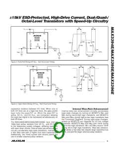
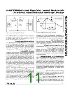
Figure 6b. ꢀꢁM Sischarge Current Waveform
Figure 6a. ꢀuman ꢁody EꢄS Test Model
To ensure full 15kV EꢄS protection, bypass V
ground with a 0.1µF ceramic capacitor and an additional
1µF ceramic capacitor as close to the device as possible.
to
CC
The high-impedance state of the I/O lines during tri-
state output mode facilitates use in multidrop networks.
In tri-state output mode, do not exceed ꢂV + 0.3Vꢃ on
L
I/O V _ or ꢂV
+ 0.3Vꢃ on I/O V _.
CC CC
L
EꢁD Test Conditions
EꢄS performance depends on a variety of conditions.
Contact Maxim for a reliability report documenting test
setup, methodology, and results.
Thermalꢂꢁhutdown -rotection
The MAX3394E/MAX3395E/MAX3396E are protected
from thermal damage resulting from short-circuit faults.
In the event of a short-circuit fault, when the junction
Applications Information
temperature ꢂT ꢃ reaches +125°C, a thermal sensor
J
forces the device into the tri-state output mode. When
-owerꢂꢁupply Decoupling
to ground with 0.1µF ceramic
CC
T drops below +115°C, normal operation resumes.
J
ꢁypass V and V
L
capacitors. To ensure full 15kV EꢄS protection,
bypass V to ground with an additional 1µF or greater
ceramic capacitor. Place all capacitors as close to the
device as possible.
±±5ꢀk EꢁD -rotection
As with all Maxim devices, EꢄS-protection structures are
incorporated on all pins to protect against EꢄS encoun-
CC
tered during handling and assembly. The I/O V _ lines
CC
are further protected by advanced EꢄS structures to
guard these pins from damage caused by EꢄS of up to
15kV. Protection structures prevent damage caused by
EꢄS events in normal operation, tri-state output mode,
and when the device is unpowered. After arresting an
EꢄS event, MAX3394E/MAX3395E/MAX3396E continue
to function without latching up, whereas competing
devices can enter a latched-up state and must be power
cycled to restore functionality.
OpenꢂDrain Mode vs. -ushꢂ-ull Mode
The MAX3394E/MAX3395E/MAX3396E are compatible
with push-pull ꢂactiveꢃ and open-drain drivers. For push-
pull operation, maximum data rate is guaranteed to
6Mbps. For open-drain applications, the MAX3394E/
MAX3395E/MAX3396E include internal pullup resistors
and slew-rate enhancement circuitry, providing a maxi-
mum data rate of 1Mbps. External pullup resistors can
be added to increase data rate when the bus is loaded
by high capacitance. ꢂꢄee the Use of External Pullup
Resistors section.ꢃ
ꢄeveral EꢄS testing standards exist for gauging the
robustness of EꢄS structures. The EꢄS protection of
the MAX3394E/MAX3395E/MAX3396E is characterized
for the human body model ꢂꢀꢁMꢃ. Figure 6a shows the
model used to simulate an EꢄS event resulting from
contact with the human body. The model consists of a
100pF storage capacitor that is charged to a high volt-
age then discharged through a 1.5kΩ resistor. Figure
6b shows the current waveform when the storage
capacitor is discharged into a low impedance.
Serial-Interface Level Translation
The MAX3395E provides level translation on four I/O
lines, making it an ideal device for multivoltage I2C,
MICROWIRE, and ꢄPI serial interfaces.
Use of External -ullup Resistors
The MAX3394E/MAX3395E/MAX3396E include internal
10kΩ pullup resistors. Suring a low-to-high logic transi-
tion, the internal pullup resistors charge the bus capac-
______________________________________________________________________________________ 11

 MAXIM [ MAXIM INTEGRATED PRODUCTS ]