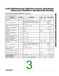
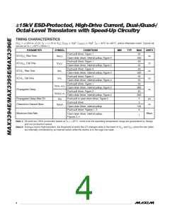
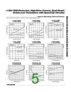
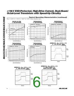
±±5ꢀk EꢁDꢂ-rotected, HighꢂDrive Current, Dualꢂ/Quadꢂ/
OctalꢂLevel Translators with ꢁpeedꢂUp Circuitry
45/MAX396E
-in Description
PIN
NAME
FUNCTION
MAX3394E
MAX3395E
MAX3396E
TDFN
UCSP
TQFN
UCSP
TQFN
UCSP
V
V
ꢄupply Voltage +1.65V ≤ V
to GNS with a 0.1µF ceramic capacitor and a
≤ +5.5V. ꢁypass
CC
CC
CC
1
2
A1
11
6
ꢁ1
14
4
S3
V
CC
1µF or greater ceramic capacitor as close to the
device as possible.
Enable Input. Srive EN logic high for normal
operation. Srive EN logic low to force all I/O lines to
a high-impedance state and disconnect internal
pullup resistors.
ꢁ1
ꢁ3
A4
EN
3
4
5
6
7
A2
A3
ꢁ3
C3
C2
10
9
C1
C2
ꢁ4
A2
A1
18
16
13
20
19
C1
S1
S4
A1
ꢁ1
I/O V
1
2
I/O 1 Referred to V
I/O 2 Referred to V
Ground
CC
CC
I/O V
CC
CC
5
GNS
I/O V 2
2
I/O 2 Referred to V
I/O 1 Referred to V
L
L
L
1
I/O V 1
L
Logic ꢄupply Voltage +1.2V ≤ V ≤ V . ꢁypass V
L
L
CC
to GNS with a 0.1µF or greater ceramic capacitor
8
C1
12
ꢁ2
3
A3
V
L
as close to the device as possible.
—
—
—
—
—
—
—
—
—
—
—
—
EP
—
—
—
—
—
—
—
—
—
—
—
—
—
3
4
A3
A4
C4
C3
—
—
—
—
—
—
—
—
—
1
2
ꢁ2
A2
S2
C2
C3
S5
C4
C5
ꢁ3
A5
ꢁ4
ꢁ5
—
I/O V 3
I/O 3 Referred to V
I/O 4 Referred to V
I/O 4 Referred to V
I/O 3 Referred to V
I/O 5 Referred to V
I/O 6 Referred to V
I/O 7 Referred to V
I/O 8 Referred to V
I/O 5 Referred to V
I/O 6 Referred to V
I/O 7 Referred to V
I/O 8 Referred to V
L
L
I/O V 4
L
L
7
15
17
12
11
10
9
I/O V
I/O V
I/O V
I/O V
I/O V
I/O V
4
3
5
6
7
8
CC
CC
CC
CC
CC
CC
CC
CC
CC
CC
CC
CC
L
8
—
—
—
—
—
—
—
—
EP
5
I/O V 5
L
6
I/O V 6
L
L
7
I/O V 7
L
L
8
I/O V 8
L
L
EP
EP
Exposed Pad. Connect exposed pad to GNS.
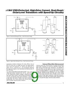
pullup resistors and increased bus load capacitance.
Externally applied voltages, V and V , set the logic-
Detailed Description
CC
L
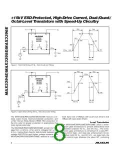
The MAX3394E/MAX3395E/MAX3396E bidirectional
level translators provide level shifting required for data
transfer in a multivoltage system. Internal slew-rate
enhancement circuitry features 10mA current-sink and
15mA current-source drivers to isolate capacitive loads
from lower current drivers. In open-drain systems, slew-
rate enhancement enables fast data rates with larger
high levels for the device. A logic-low signal on one I/O
side of the device appears as a logic-low signal on the
opposite I/O side and vice-versa. Each I/O line is pulled
up to V
or V by an internal pullup resistor, allowing
L
CC
the devices to be driven by either push-pull or open-
drain drivers.
_______________________________________________________________________________________
7

 MAXIM [ MAXIM INTEGRATED PRODUCTS ]