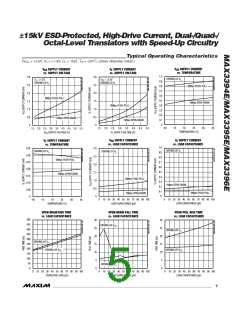
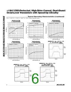
±±5ꢀk EꢁDꢂ-rotected, HighꢂDrive Current, Dualꢂ/Quadꢂ/
OctalꢂLevel Translators with ꢁpeedꢂUp Circuitry
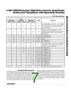
45/MAX396E
t
t
FVL
RVL
V
V
L
CC
I/O V
CC
EN
V
V
CC
L
MAX3394E
MAX3395E
MAX3396E
V
V
CC
L
90%
90%
50%
50%
50%
50%
I/O V
CC_
I/O V
L_
10%
50Ω
10%
t
I/O V
L
C
IOVL
t
I/OVCC-VL
I/OVCC-VL
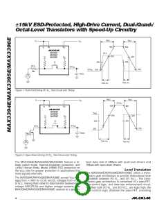
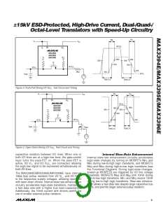
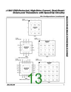
Figure 3. Push-Pull Sriving I/O V
Test Circuit and Timing
CC_
t
t
RVL
V
L
V
FVL
CC
EN
V
V
L
CC
I/O V
L
MAX3394E
MAX3395E
MAX3396E
90%
90%
50%
50%
V
V
CC
L
50%
50%
I/O V
10%
10%
I/O V
CC_
L_
C
IOVL
V
GATE
t
t
I/OVCC-VL
I/OVCC-VL
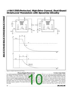
Figure 4. Open-Srain Sriving I/O V
Test Circuit and Timing
CC_
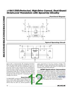
capacitive isolation between I/O lines. When one or
both I/O lines are at a logic-low level, the gate-control
logic turns the pass-FET on. When the pass-FET is
active, I/O V _ and I/O V _ are connected, allowing
the logic-low signal to be expressed simultaneously on
both I/O lines.
Internal ꢁlewꢂRate Enhancement
Internal slew-rate enhancement circuitry accelerates
logic-state changes by turning on MOꢄFETs M and
P1
M
M
during low-to-high logic transitions, and MOꢄFETs
L
CC
P2
N3
and M
during high-to-low logic transitions ꢂsee
N4
the Functional Siagramꢃ. Suring logic-state changes,
speed-up MOꢄFETꢄ are triggered by I/O line voltage
thresholds. MOꢄFETꢄ M
high-to-low logic transitions. M and M source 15mA
The MAX3394E/MAX3395E/MAX3396E have internal
and M
sink 10mA during
N3
N4
10kΩ ꢂtypꢃ pullup resistors from I/O V _ and I/O V
_
L
CC
P1
P2
to the respective supply voltages, allowing operation
with open-drain drivers. Internal slew-rate enhancement
circuitry accelerates logic-state transitions, maintaining
a fast data rate with a higher bus load capacitance.
Additionally, the 10mA current sink drivers permit the
use of smaller external pullup resistors.
during low-to-high logic transitions. ꢄlew-rate enhance-
ment allows a fast data rate despite large capacitive bus
loads, and permits larger external pullup resistors.
_______________________________________________________________________________________
9

 MAXIM [ MAXIM INTEGRATED PRODUCTS ]