Low-Cost Multichemistry Battery Chargers
where dV is the maximum voltage sag of 0.5V while
delivering energy to the inductor during the high-side
MOSFET on-time, and dt is the period at highest oper-
ating frequency (400kHz):
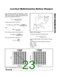
the MOSFET. Choose N1b with either an internal
Schottky diode or body diode capable of carrying the
maximum charging current during the dead time. The
Schottky diode D3 provides the supply current to the
high-side MOSFET driver.
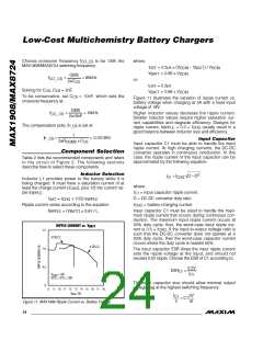
I
2.5µs
C1
C1>
×
Layout and Bypassing
2
0.5V
Bypass DCIN with a 1µF capacitor to power ground
(Figure 1). D2 protects the MAX1908/MAX8724 when
the DC power source input is reversed. A signal diode
for D2 is adequate because DCIN only powers the
MAX1908 internal circuitry. Bypass LDO, REF, CCV,
CCI, CCS, ICHG, and IINP to analog ground. Bypass
DLOV to power ground.
Both tantalum and ceramic capacitors are suitable in
most applications. For equivalent size and voltage
rating, tantalum capacitors have higher capacitance,
but also higher ESR than ceramic capacitors. This
makes it more critical to consider ripple current and
power-dissipation ratings when using tantalum capaci-
tors. A single ceramic capacitor often can replace two
tantalum capacitors in parallel.
Good PC board layout is required to achieve specified
noise, efficiency, and stable performance. The PC
board layout artist must be given explicit instructions—
preferably, a pencil sketch showing the placement of
the power-switching components and high-current rout-
ing. Refer to the PC board layout in the MAX1908 eval-
uation kit for examples. Separate analog and power
grounds are essential for optimum performance.
Output Capacitor
The output capacitor absorbs the inductor ripple cur-
rent. The output capacitor impedance must be signifi-
cantly less than that of the battery to ensure that it
absorbs the ripple current. Both the capacitance and
ESR rating of the capacitor are important for its effec-
tiveness as a filter and to ensure stability of the DC-DC
converter (see the Compensation section). Either tanta-
lum or ceramic capacitors can be used for the output
filter capacitor.
Use the following step-by-step guide:
1) Place the high-power connections first, with their
grounds adjacent:
MOSFETs and Diodes
Schottky diode D1 provides power to the load when the
AC adapter is inserted. This diode must be able to
deliver the maximum current as set by RS1. For
reduced power dissipation and improved dropout per-
formance, replace D1 with a P-channel MOSFET (P1)
as shown in Figure 2. Take caution not to exceed the
a) Minimize the current-sense resistor trace lengths,
and ensure accurate current sensing with Kelvin
connections.
b) Minimize ground trace lengths in the high-current
paths.
c) Minimize other trace lengths in the high-current
paths.
maximum V
limit the V
of P1. Choose resistors R11 and R12 to
GS
.
d) Use > 5mm wide traces.
GS
The N-channel MOSFETs (N1a, N1b) are the switching
devices for the buck controller. High-side switch N1a
should have a current rating of at least the maximum
charge current plus one-half the ripple current and
e) Connect C1 to high-side MOSFET (10mm max
length).
f) LX node (MOSFETs, inductor (15mm max
length)).
have an on-resistance (R
) that meets the power
DS(ON)
Ideally, surface-mount power components are flush
against one another with their ground terminals
almost touching. These high-current grounds are
then connected to each other with a wide, filled zone
of top-layer copper, so they do not go through vias.
dissipation requirements of the MOSFET. The driver for
N1a is powered by BST. The gate-drive requirement for
N1a should be less than 10mA. Select a MOSFET with a
low total gate charge (Q
) and determine the
GATE
required drive current by I
= Q
× f (where f is
GATE
GATE
the DC-DC converter’s maximum switching frequency).
The resulting top-layer power ground plane is
connected to the normal ground plane at the
MAX1908/MAX8724s’ backside exposed pad.
Other high-current paths should also be minimized,
but focusing primarily on short ground and current-
sense connections eliminates most PC board lay-
out problems.
The low-side switch (N1b) has the same current rating
and power dissipation requirements as N1a, and
should have a total gate charge less than 10nC. N2 is
used to provide the starting charge to the BST capacitor
(C15). During the dead time (50ns, typ) between N1a
and N1b, the current is carried by the body diode of
______________________________________________________________________________________ 25

 MAXIM [ MAXIM INTEGRATED PRODUCTS ]