MAX17047/MAX17050
ModelGauge m3 Fuel Gauge
range. The resulting data is placed in the V
every 175.8ms with an LSb value of 0.625mV. Voltages
above the maximum register value are reported as the
register
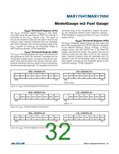
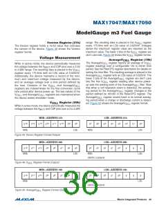
Version Register (21h)
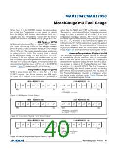
The Version register holds a 16-bit value that indicates
the version of the device. Figure 48 shows the Version
register format.
CELL
maximum value. The lower 3 bits of the V
register are
CELL
register format.
don’t care bits. Figure 49 shows the V
CELL
Voltage Measurement
AverageV
Register (19h)
CELL
The AverageV
register reports an average of V
CELL
CELL
While in active mode, the device periodically measures
register readings over a configurable 12s to 24min time
period. See the FilterCFG register description for details on
setting the time filter. The resulting average is placed in the
the voltage between the V
to 4.98V range. The resulting data is placed in the V
and CSP pins over a 2.5V
BATT
CELL
register every 175.8ms with an LSb value of 0.625mV.
Additionally, the device maintains a record of the mini-
mum and maximum voltage measured by the device,
and an average voltage over a time period defined by
AverageV
register with an LSb value of 0.625mV. The
CELL
lower 3 bits of the AverageV
register are don’t care
CELL
bits.The first V
register reading after device power-
CELL
up sets the starting point of the AverageV
filter. Note
CELL
the host. Contents of the V
and AverageV
CELL
CELL
that when a cell relaxation event is detected, the averag-
ing period for the AverageV register changes to the
registers are indeterminate for the first conversion cycle
time period after device power-up. The last values of the
CELL
period defined by dt3:dt0 in the RelaxCFG register. The
AverageV register reverts back to its normal averag-
V
CELL
and AverageV
registers are maintained when
CELL
CELL
the device enters shutdown mode.
ing period when a charge or discharge current is detect-
ed. Figure 50 shows the AverageV register format.
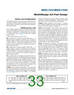
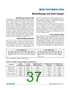
V
Register (09h)
CELL
CELL
While in active mode, the device periodically measures the
voltage between the V and CSP pins over a 0 to 4.98V
BATT
MSB—ADDRESS 21h
LSB—ADDRESS 21h
15
14
13
12
11
10
9
8
7
6
5
4
3
2
1
0
V
V
V
V
V
V
V
V
V
V
V
V
V
V
V
V
MSb
Figure 48. Version Register Format (Output)
LSb
MSb
LSb
MSB—ADDRESS 09h
LSB—ADDRESS 09h
12
11
10
9
8
7
6
5
4
3
2
1
0
2
2
2
2
2
2
2
2
2
2
2
2
2
X
X
X
MSb
LSb
MSb
LSb
UNITS: 0.625mV
Figure 49. V
Register Format (Output)
CELL
MSB—ADDRESS 19h
LSB—ADDRESS 19h
12
2
11
10
9
8
7
6
5
4
3
2
1
0
2
2
2
2
2
2
2
2
2
2
2
2
X
X
X
MSb
LSb
MSb
UNITS: 0.625mV
LSb
Figure 50. AverageV
Register Format (Output)
CELL
���������������������������������������������������������������� Maxim Integrated Products 36

 MAXIM [ MAXIM INTEGRATED PRODUCTS ]