MAX11329–MAX11332
3Msps, 12-/10-Bit, 8-/16-Channel ADCs with
Post-Mux External Signal Conditioning Access
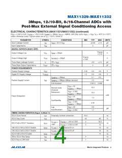
ELECTRICAL CHARACTERISTICS (MAX11329/MAX11330) (continued)
(V
= 2.35V to 3.6V, V
= 1.5V to 3.6V, f
= 3Msps, f
= 48MHz, 50% duty cycle, V
= V , T = -40NC to +125NC,
DD
OVDD
SAMPLE
SCLK
REF+ DD A
unless otherwise noted. Typical values are at T = +25NC.) (Note 2)
A
PARAMETER
SYMBOL
CONDITIONS
MIN
1
TYP
MAX
UNITS
ns
SCLK Rise to DIN Hold
t
DH
t
4
ns
CS Fall to SCLK Fall Setup
SCLK Fall to CS Fall Hold
CNVST Pulse Width
CSS
t
1
ns
CSH
t
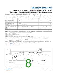
See Figure 6
5
ns
CSW
CS or CNVST Rise to EOC Low
(Note 7)
t
See Figure 7, f
= 3Msps
1.7
2.4
Fs
CNV_INT
SAMPLE
t
5
ns
CS Pulse Width
CSBW
Note 2: Limits are 100% production tested at T = +25NC. Limits over the operating temperature range are guaranteed by design.
A
Parts are tested with MUX externally connected to the ADC input.
Note 3: Channel ID disabled.
Note 4: Tested in single-ended mode.
Note 5: Offset nulled.
Note 6: Line rejection D(D
) with V
= 2.35V to 3.6V and V
= 2.35V.
OUT
DD
REF+
Note 7: Tested and guaranteed with fully differential input.
Note 8: Conversion time is defined as the number of clock cycles multiplied by the clock period with a 50% duty cycle.
Maximum conversion time: 1.91Fs + N x 16 x t
OSC_MAX
t
= 29.4ns, t
= 25ns.
OSC_MAX
OSC_TYP
Note 9: The operational input voltage range for each individual input of a differentially configured pair is from V
to GND. The
DD
operational input voltage difference is from -V
Note 10: See Figure 3 (Equivalent Input Circuit).
Note 11: Guaranteed by characterization.
/2 to +V
/2 or -V
to +V
.
REF+
REF+
REF+
REF+
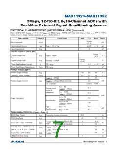
t
CSBW
CS
t
t
t
CP
CSH
CSS
t
CH
1ST
CLOCK
SCLK
16TH
CLOCK
t
DH
t
DS
t
DOT
DIN
t
DOD
t
DOE
DOUT
Figure 1. Detailed Serial-Interface Timing Diagram
����������������������������������������������������������������� Maxim Integrated Products
8

 MAXIM [ MAXIM INTEGRATED PRODUCTS ]