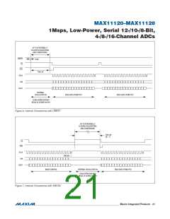
MAX11120–MAX11128
1Msps, Low-Power, Serial 12-/10-/8-Bit,
4-/8-/16-Channel ADCs
OUTPUT CODE (hex)
OUTPUT CODE (hex)
V
REF+
+FS =
ZS = 0
-FS =
FFF
FFE
FFD
FFC
FFB
FS = V
REF+
7FF
7FE
2
ZS = 0
-V
REF+
V
REF+
1 LSB =
2
4096
V
REF+
1 LSB =
001
000
FFF
FFE
4096
004
003
002
001
000
801
800
0
1
2
3
4
FS
-FS
0
+FS
FS -1.5 LSB
INPUT VOLTAGE (LSB)
-FS +0.5 LSB
+FS -1.5 LSB
INPUT VOLTAGE (LSB)
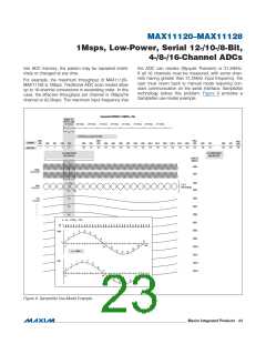
Figure 4. Unipolar Transfer Function for 12-Bit Resolution
Figure 5. Bipolar Transfer Function for 12-Bit Resolution
Control register (Table 2). The wake-up, acquisition, con-
version, and shutdown sequences are initiated through
CNVST and are performed automatically using the inter-
nal oscillator. Results are added to the internal FIFO.
Internal FIFO
The MAX11120–MAX11128 contain a FIFO buffer that can
hold up to 16 ADC results. This allows the ADC to handle
multiple internally clocked conversions without tying up
the serial bus. If the FIFO is filled and further conversions
are requested without reading from the FIFO, the oldest
ADC results are overwritten by the new ADC results. Each
result contains 2 bytes, with the MSB preceded by four
leading channel address bits. After each falling edge of
CS, the oldest available byte of data is available at DOUT.
When the FIFO is empty, DOUT is zero.
With CS high, initiate a scan by setting CNVST low for
at least 5ns before pulling it high (Figure 6). Then, the
MAX11120–MAX11128 wake up, scan all requested
channels, store the results in the FIFO, and shut down.
After the scan is complete, EOC is pulled low and the
results are available in the FIFO. Wait until EOC goes
low before pulling CS low to communicate with the serial
interface. EOC stays low until CS or CNVST is pulled low
again. Do not initiate a second CNVST before EOC goes
low; otherwise, the FIFO may become corrupted.
External Clock
In external clock mode, the analog inputs are sampled at
the falling edge of CS. Serial clock (SCLK) is used to per-
form the conversion. The sequencer reads in the channel
to be converted from the serial data input (DIN) at each
frame. The conversion results are sent to the serial output
(DOUT) at the next frame.
Alternatively, set SWCNV to 1 in the ADC Mode Control
register to initiate conversions with CS rising edge
instead of cycling CNVST (Table 2). For proper operation,
CS must be held low for 17 clock cycles to guarantee
that the device interprets the SWCNV setting. A delay
is initiated at the rising edge of CS and the conversion
is started when the delay times out. Upon completing
the conversion, this bit is reset to 0 (Figure 7). Apply a
soft reset when changing from internal to external clock
mode: RESET[1:0] = 10.
Internal Clock
The MAX11120–MAX11128 operate from an internal
oscillator, which is accurate within Q15% of the 13.33MHz
nominal clock rate. Request internally timed conversions
by writing the appropriate sequence to the ADC Mode
���������������������������������������������������������������� Maxim Integrated Products 20

 MAXIM [ MAXIM INTEGRATED PRODUCTS ]