MAX11120–MAX11128
1Msps, Low-Power, Serial 12-/10-/8-Bit,
4-/8-/16-Channel ADCs
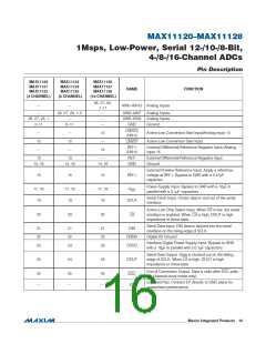
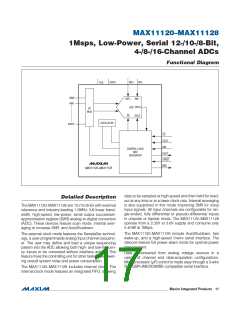
Functional Diagram
V
DD
OVDD
REF+ REF-
AIN0
AIN1
REF+
ADC
CS
REF-
DOUT
SCLK
I/P
MUX
OSCILLATOR
AIN15
CS
SCLK
DIN
CONTROL LOGIC
AND
SEQUENCER
DOUT
CNVST
EOC
MAX11120–MAX11128
data to be sampled at high speed and then held for read-
out at any time or at a lower clock rate. Internal averaging
is also supported in this mode improving SNR for noisy
input signals. All input channels are configurable for sin-
gle-ended, fully differential or pseudo-differential inputs
in unipolar or bipolar mode. The MAX11120–MAX11128
operate from a 2.35V to 3.6V supply and consume only
5.4mW at 1Msps.
Detailed Description
The MAX11120–MAX11128 are 12-/10-/8-bit with external
reference and industry-leading 1.5MHz, full linear band-
width, high-speed, low-power, serial output successive-
approximation register (SAR) analog-to-digital converters
(ADC). These devices feature scan mode, internal aver-
aging to increase SNR, and AutoShutdown.
The MAX11120–MAX11128 include AutoShutdown, fast
wake-up, and a high-speed 3-wire serial interface. The
devices feature full power-down mode for optimal power
management.
The external clock mode features the SampleSet technol-
ogy, a user-programmable analog input channel sequenc-
er. The user may define and load a unique sequencing
pattern into the ADC allowing both high- and low-frequen-
cy inputs to be converted without interface activity. This
feature frees the controlling unit for other tasks while lower-
ing overall system noise and power consumption.
Data is converted from analog voltage sources in a
variety of channel and data-acquisition configurations.
Microprocessor (FP) control is made easy through a 3-wire
SPI-/QSPI-/MICROWIRE-compatible serial interface.
The MAX11120–MAX11128 includes internal clock. The
internal clock mode features an integrated FIFO, allowing
���������������������������������������������������������������� Maxim Integrated Products 17

 MAXIM [ MAXIM INTEGRATED PRODUCTS ]