MAX11120–MAX11128
1Msps, Low-Power, Serial 12-/10-/8-Bit,
4-/8-/16-Channel ADCs
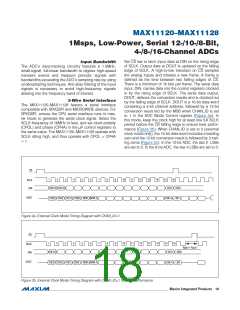
Set CS low to latch input data at DIN on the rising edge
of SCLK. Output data at DOUT is updated on the falling
edge of SCLK. A high-to-low transition on CS samples
the analog inputs and initiates a new frame. A frame is
defined as the time between two falling edges of CS.
There is a minimum of 16 bits per frame. The serial data
input, DIN, carries data into the control registers clocked
in by the rising edge of SCLK. The serial data output,
DOUT, delivers the conversion results and is clocked out
by the falling edge of SCLK. DOUT is a 16-bit data word
containing a 4-bit channel address, followed by a 12-bit
conversion result led by the MSB when CHAN_ID is set
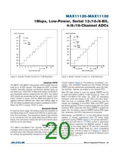
to 1 in the ADC Mode Control register (Figure 2a). In
this mode, keep the clock high for at least one full SCLK
period before the CS falling edge to ensure best perfor-
mance (Figure 2b). When CHAN_ID is set to 0 (external
clock mode only), the 16-bit data word includes a leading
zero and the 12-bit conversion result is followed by 3 trail-
ing zeros (Figure 2c). In the 10-bit ADC, the last 2 LSBs
are set to 0. In the 8-bit ADC, the last 4 LSBs are set to 0.
Input Bandwidth
The ADC’s input-tracking circuitry features a 1.5MHz,
small-signal, full-linear bandwidth to digitize high-speed
transient events and measure periodic signals with
bandwidths exceeding the ADC’s sampling rate by using
undersampling techniques. Anti-alias filtering of the input
signals is necessary to avoid high-frequency signals
aliasing into the frequency band of interest.
3-Wire Serial Interface
The MAX11120–MAX11128 feature a serial interface
compatible with SPI/QSPI and MICROWIRE devices. For
SPI/QSPI, ensure the CPU serial interface runs in mas-
ter mode to generate the serial clock signal. Select the
SCLK frequency of 16MHz or less, and set clock polarity
(CPOL) and phase (CPHA) in the FP control registers to
the same value. The MAX11120–MAX11128 operate with
SCLK idling high, and thus operate with CPOL = CPHA
= 1.
CS
1
2
3
4
5
6
7
8
9
10
11
12
13
14
15
16
SCLK
DIN
DI[15] DI[14]
DI[1] DI[0]
DOUT
Ch[3] Ch[2] Ch[1] Ch[0] MSB MSB-1
LSB+1 LSB
Figure 2a. External Clock Mode Timing Diagram with CHAN_ID=1
CS
1
2
3
4
5
6
7
8
9
10
11
12
13
14
15
16
SCLK
DIN
t
> t
QUIET SCLK
DI[15]
DI[1] DI[0]
DOUT
Ch[3] Ch[2] Ch[1] Ch[0] MSB MSB-1
LSB+1 LSB
Figure 2b. External Clock Mode Timing Diagram with CHAN_ID=1 for Best Performance
���������������������������������������������������������������� Maxim Integrated Products 18

 MAXIM [ MAXIM INTEGRATED PRODUCTS ]