MAX11120–MAX11128
1Msps, Low-Power, Serial 12-/10-/8-Bit,
4-/8-/16-Channel ADCs
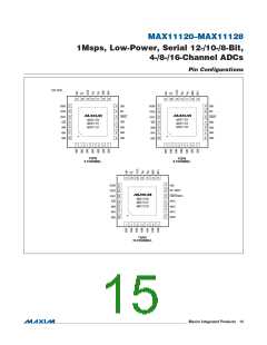
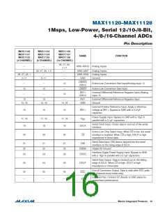
Pin Description
MAX11120
MAX11121
MAX11122
MAX11123
MAX11124
MAX11125
MAX11126
MAX11127
MAX11128
NAME
FUNCTION
(4 CHANNEL)
(8 CHANNEL)
(16 CHANNEL)
26, 27, 28,
1–11
—
—
AIN0–AIN13 Analog Inputs
—
26, 27, 28, 1–5
—
AIN0–AIN7
AIN0–AIN3
GND
Analog Inputs
Analog Inputs
Ground
26, 27, 28, 1
2–11
—
—
—
6–11
CNVST/
AIN14
—
12
—
—
12
—
12
—
13
Active-Low Conversion Start Input/Analog Input 14
Active-Low Conversion Start Input
CNVST
REF-/
AIN15
External Differential Reference Negative Input /Analog
Input 15
13
13
—
REF-
GND
External Differential Reference Negative Input
Ground
14, 16
14, 16
14, 16
External Positive Reference Input. Apply a reference
voltage at REF+. Bypass to GND with a 0.47FF
capacitor.
15
15
15
REF+
Power-Supply Input. Bypass to GND with a 10FF in
parallel with a 0.1FF capacitors.
17, 18
19
17, 18
19
17, 18
19
V
DD
Serial Clock Input. Clocks data in and out of the serial
interface
SCLK
Active-Low Chip Select Input. When CS is low, the serial
interface is enabled. When CS is high, DOUT is high
impedance or three-state.
20
20
20
CS
Serial Data Input. DIN data is latched into the serial
interface on the rising edge of SCLK.
21
22
23
21
22
23
21
22
23
DIN
DGND
OVDD
Digital I/O Ground
Interface Digital Power-Supply Input. Bypass to GND
with a 10FF in parallel with a 0.1FF capacitors.
Serial Data Output. Data is clocked out on the falling
edge of SCLK. When CS is high, DOUT is high
impedance or three-state.
24
24
24
DOUT
End of Conversion Output. Data is valid after EOC pulls
low (Internal clock mode only).
25
—
25
—
25
—
EOC
Exposed Pad. Connect EP directly to GND plane for
guaranteed performance.
EP
���������������������������������������������������������������� Maxim Integrated Products 16

 MAXIM [ MAXIM INTEGRATED PRODUCTS ]