MAX11120–MAX11128
1Msps, Low-Power, Serial 12-/10-/8-Bit,
4-/8-/16-Channel ADCs
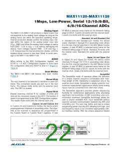
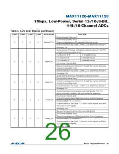
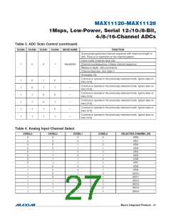
Averaging Mode
In averaging mode, the device performs the specified
Register Descriptions
number of conversions and returns the average for each
requested result in the FIFO. The averaging mode works
with internal clock only.
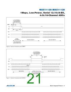
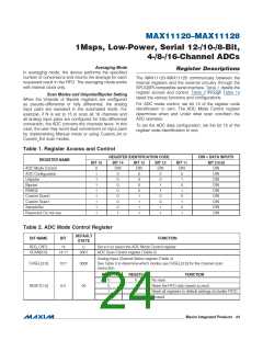
The MAX11120–MAX11128 communicate between the
internal registers and the external circuitry through the
SPI-/QSPI-compatible serial interface. Table 1 details the
register access and control. Table 2 through Table 14
detail the various functions and configurations.
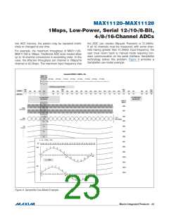
Scan Modes and Unipolar/Bipolar Setting
When the Unipolar or Bipolar registers are configured
as pseudo-differential or fully differential, the analog
input pairs are repeated in this automated mode. For
example, if N is set to 15 to scan all 16 channels and
all analog input pairs are configured for fully-differential
conversion, the ADC converts the channels twice. In this
case, the user may avoid dual conversions on input pairs
by implementing Manual mode or using Custom_Int or
Custom_Ext scan modes.
For ADC mode control, set bit 15 of the register code
identification to zero. The ADC Mode Control register
determines when and under what scan condition the
ADC operates.
To set the ADC data configuration, set the bit 15 of the
register code identification to one.
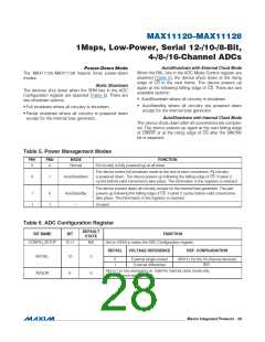
Table 1. Register Access and Control
REGISTER IDENTIFICATION CODE
DIN ≡ DATA INPUTS
REGISTER NAME
BIT 15
BIT 14
BIT 13
BIT 12
BIT 11
BIT [10:0]
DIN
ADC Mode Control
ADC Configuration
Unipolar
0
1
1
1
1
1
1
1
1
DIN
0
DIN
0
DIN
0
DIN
0
DIN
0
0
0
1
DIN
Bipolar
0
0
1
0
DIN
RANGE
0
0
1
1
DIN
Custom Scan0
Custom Scan1
SampleSet
0
1
0
0
DIN
0
1
0
1
DIN
0
1
1
0
DIN
Reserved. Do not use.
1
1
1
1
DIN
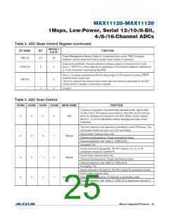
Table 2. ADC Mode Control Register
DEFAULT
STATE
BIT NAME
BIT
FUNCTION
REG_CNTL
SCAN[3:0]
15
0
Set to 0 to select the ADC Mode Control register
ADC Scan Control register (Table 3)
14:11
0001
Analog Input Channel Select register (Table 4).
CHSEL[3:0]
10:7
6:5
0000
See Table 3 to determine which modes use CHSEL[3:0] for the channel scan
instruction.
RESET1
RESET0
FUNCTION
0
0
1
1
0
1
0
1
No reset
RESET[1:0]
00
Reset the FIFO only (resets to zero)
Reset all registers to default settings (includes FIFO)
Unused
���������������������������������������������������������������� Maxim Integrated Products 24

 MAXIM [ MAXIM INTEGRATED PRODUCTS ]