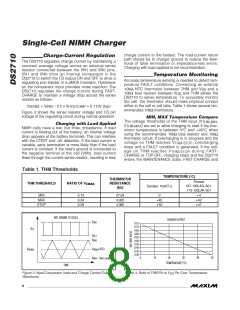
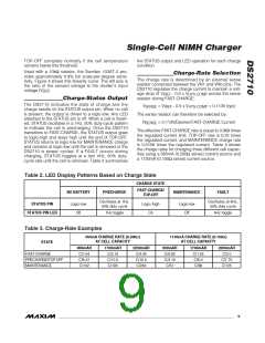
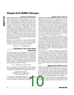
Single-Cell NiMH Charger
CONTROL
R
GATE
L
SWITCH
Q
SWITCH
LOOP1
LOOP2
DS2710
C
IN
D
C
OUT
CHARGE SOURCE SIDE
BATTERY SIDE
SWITCH
LOOP AREAS MINIMIZED
CHARGE SOURCE SIDE
BATTERY SIDE
C
I
D
S
C
O
Q
S
L
S
R
G
BACKSIDE
GROUND PLANE
CONTROL
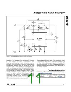
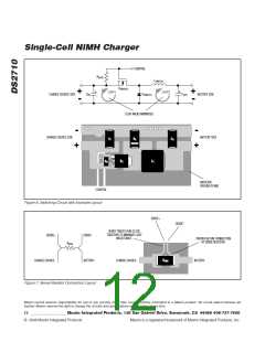
Figure 6. Switching Circuit with Example Layout
SENSE+
SENSE-
SENSE TRACES RUN CLOSE
TOGETHER TO MINIMIZE LOOP
INDUCTANCE
SENSE+
SENSE-
PROPER KELVIN CONNECTION
AT SENSE RESISTOR
R
SNS
R
SNS
CHARGE SOURCE-
BATTERY-
CHARGE SOURCE-
BATTERY-
Figure 7. Sense Resistor Connection Layout
Maxim cannot assume responsibility for use of any circuitry other than circuitry entirely embodied in a Maxim product. No circuit patent licenses are
implied. Maxim reserves the right to change the circuitry and specifications without notice at any time.
12 ____________________Maxim Integrated Products, 120 San Gabriel Drive, Sunnyvale, CA 94086 408-737-7600
© 2008 Maxim Integrated Products
Maxim is a registered trademark of Maxim Integrated Products, Inc.

 MAXIM [ MAXIM INTEGRATED PRODUCTS ]