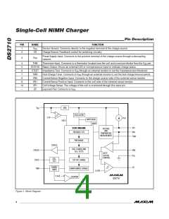
Single-Cell NiMH Charger
DS2710
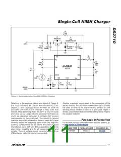
R3
270kΩ
Q1
ZXM62P02E6
L1
15μH
SISCDRH74M-150R
+5V
(USB+)
C2
10μF
CERAMIC
D2
C3
10μF
CERAMIC
R1
150Ω
1W B340A-13
SCHOTTKY
R6
1kΩ
CS
V
VP1
VN1
VN0
DD
1S
NiMH
CELL
R4
10kΩ
THM
DS2710
C1
1μF
R9
0.1Ω
1W
STATUS
RT1
103AT-2
TMR
CTEST
V
SS
R2
1kΩ
R7
100kΩ
R8
47kΩ
D1
GREEN
SMA
GROUND
(USB-)
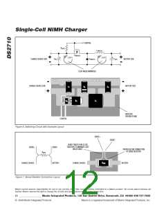
Figure 5. Typical Application Circuit for USB Port Charging
Referring to the example circuit and layout of Figure 6,
the loop labeled as Loop1 encompassing C
Another important layout detail is the connection of the
sense resistor. Proper Kelvin connection layout should
be used to ensure the signal quality viewed by the
sensing circuit inside the DS2710 is adequate. Figure 7
shows a recommended connection of the sense lines to
the resistor footprint.
,
IN
Q
, and D
should be kept as small as
SWITCH
SWITCH
possible to minimize the change in loop area that
occurs when switching from the OFF to the ON state
and vice versa. Loop2 should also be minimized as
much as practical, although it contains DC current
components for the most part. The returning ground
currents should be allowed to follow a path on a layer
directly under the outgoing path since the high-fre-
quency components try to follow the path of least
impedance. Low ESR and ESL capacitors should be
used when possible and for all capacitors 10µF and
smaller. Typical surface-mount ceramic types with an
X5R or better dielectric are recommended.
Package Information
For the latest package outline information and land patterns, go
to www.maxim-ic.com/packages.
PACKAGE TYPE PACKAGE CODE DOCUMENT NO.
10 TDFN-EP
T1034+1
21-0268
______________________________________________________________________________________ 11

 MAXIM [ MAXIM INTEGRATED PRODUCTS ]