Single-Cell NiMH Charger
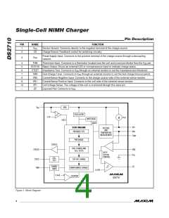
Pin Description
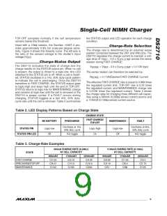
PIN
1
NAME
FUNCTION
V
Device Ground. Connects directly to the negative terminal of the charge source.
Charge Source. Feedback control for switching circuitry.
SS
2
CS
Power-Supply Input. Connects to the positive terminal of the charge source through a decoupling
network.
3
V
DD
DS2710
4
5
THM
Thermistor Input. Connects to a thermistor located near the cell and a resistor-divider from the V pin.
DD
STATUS Status Output. Drives an external LED or microprocessor input to indicate charge status.
6
CTEST
TMR
VN0
VN1
VP1
Impedance Test. Connects to V through an external resistor to set the impedance-test threshold.
SS
7
Fast-Charge Timer. Connects to V through an external resistor to set the fast-charge timeout period.
SS
8
Current-Sense Negative Input. Connects to the charge source side of the external sense resistor.
Current-Sense Positive Input. Connects to the cell side of the external sense resistor.
Cell Voltage Sense. The voltage of the cell is monitored through this input pin.
9
10
—
EP
Exposed Pad. Connects to V
.
SS
V
BIAS
DD
OSCILLATOR
3.5V
I
PTST
WATCHDOG
ABORT
UVLO
VP1
VN1
THM
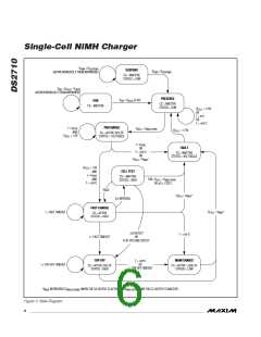
STATE MACHINE
VOLTAGE
AND
TEMPERATURE
MEASUREMENT
PRESENSE TEST
PRECHARGE
STATUS
FAST-CHARGE AND
CELL TESTS
STATUS
VN0
DUTY-
FACTOR
CONTROL
V
SS
CELL
TEST
CTEST
TMR
TOP-OFF CHARGE
CHARGE
TIMER
CS
MAINTENANCE CHARGE
SUSPEND
0.125V
0.1μA
DS2710
Figure 1. Block Diagram
4
_______________________________________________________________________________________

 MAXIM [ MAXIM INTEGRATED PRODUCTS ]