71M6543F/H and 71M6543G/GH Data Sheet
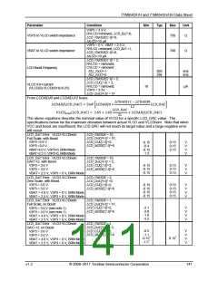
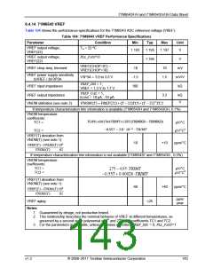
Parameter
Condition
Min
Typ
Max
Unit
LCD_DAC Error. VLCD-VLCDnom
Zero Scale, no Boost
V3P3 = 3.6 V
LCD_VMODE = 01,
LCD_DAC[4:0] = 0,
LCD_CLK[1:0]=2,
LCD_MODE[2:0]=6
-0.15
-0.15
-0.15
-0.45
0.15
0.15
0.15
0.15
V
V
V
V
V3P3 = 3.0 V
VBAT = 4.0 V, V3P3 = 0 V, BRN Mode
VBAT = 2.5 V, V3P3 = 0 V, BRN Mode
LCD_DAC Error. VLCD-VLCDnom
Full Scale, with Boost, LCD mode
VBAT = 4.0 V, V3P3 = 0 V
VBAT = 2.5 V, V3P3 = 0 V
Note:
LCD_VMODE = 1,
LCD_DAC[4:0] = 1F,
LCD_CLK[1:0]=2,
LCD_MODE[2:0]=6
-0.15
-1.3
0.15
V
V
1. Guaranteed by design; not production tested.
2. The following test conditions also apply to all parameters provided in this table: bypass capacitor CVLCD ≥
0.1 µF, test load RVLCD = 500 kΩ, no display, all SEGDIO pins configured as DIO.
142
© 2008–2011 Teridian Semiconductor Corporation
v1.2

 MAXIM [ MAXIM INTEGRATED PRODUCTS ]