71M6543F/H and 71M6543G/GH Data Sheet
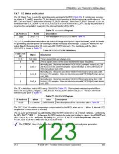
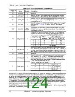
Table 78: CECONFIG Bit Definitions (CE RAM 0x20)
Default Description
CECONFIG
Name
Reserved
bit
23
0
0
Reserved.
When 1, the MPU controls temperature compensation via the
GAIN_ADJn (CE RAM 0x40-0x42), when 0, the CE is in control.
EXT_TEMP
22
When 1, XPULSE produces a pulse for each zero-crossing of
the mains phase selected by FREQSEL[1:0] , which can be used
to interrupt the MPU.
EDGE_INT
SAG_INT
21
20
1
1
When 1, activates the YPULSE/SEGDIO7 output when a sag is
detected (see 2.5.10) on the phase selected with FREQ-
SEL[1:0].
The number of consecutive voltage samples below SAG_THR
(CE RAM 0x24) before a sag alarm is declared. The default value
is equivalent to 100 ms.
218
(0xDA)
SAG_CNT
19:8
FREQSEL[1:0] selects the phase to be used for the frequency
monitor, sag detection, the phase-to-phase lag calculation and
for the zero crossing counter (MAINEDGE_X, CE RAM 0x83).
Phase
Selected
Phases Selected
PH_AtoB_X PH_AtoC_X
FREQ SEL[1:0]
FREQSEL[1:0]
7:6
0
0
0
1
1
0
1
0
1
A
B
C
A-B
B-C
A-C
B-A
C-B
C-A
Not allowed
When zero, causes the pulse generators to respond to internal
data. WPULSE = WSUM_X (CE RAM 0x84), VPULSE = VARSUM_X
(CE RAM 0x88.) Otherwise, the generators respond to values the
MPU places in APULSEW and APULSER (CE RAM 0x45 and 0x49)
EXT_PULSE
Reserved
5
1
0
4:2
Reserved.
When PULSE_FAST = 1, the pulse generator input is increased
16x. When PULSE_SLOW = 1, the pulse generator input is
reduced by a factor of 64. These two parameters control the
pulse gain factor X (see table below). Allowed values are either
1 or 0. Default is 0 for both (X = 6).
PULSE_FAST
1
0
PULSE_FAST PULSE_SLOW
X
0
0
1
1
0
1
0
1
1.5 * 22 = 6
1.5 * 2-4 = 0.09375
1.5 * 26 = 96
Do not use
PULSE_SLOW
0
0
The FREQSEL[1:0] field in CECONFIG (CE RAM 0x20[7:6]) selects the phase that is utilized to generate a sag
interrupt. Thus, a SAG_INT event occurs when the selected phase has satisfied the sag event criteria as
set by the SAG_THR (CE RAM 0x24) register and the SAG_CNT field in CECONFIG (CE RAM 0x20[19:8]).
When the SAG_INT bit (CE RAM 0x20[20]) is set to 1, a sag event generates a transition on the YPULSE
output. After a sag interrupt, the MPU should change the FREQSEL[1:0] setting to select the other phase,
if it is powered. Even though a sag interrupt is only generated on the selected phase, all three phases
are simultaneously checked for sag. The presence of power on a given phase can be sensed by directly
checking the SAG_A, SAG_B and SAG_C bits in CESTATUS (CE RAM 0x80[0:1]).
The EXT_TEMP bit enables temperature compensation by the MPU, when set to 1. When 0, internal (CE)
temperature compensation is enabled.
124
© 2008–2011 Teridian Semiconductor Corporation
v1.2

 MAXIM [ MAXIM INTEGRATED PRODUCTS ]