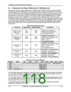
71M6543F/H and 71M6543G/GH Data Sheet
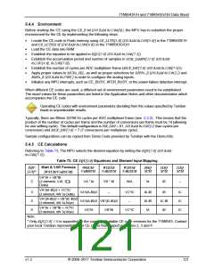
5.4.6 CE Front-End Data (Raw Data)
Access to the raw data provided by the AFE is possible by reading CE RAM addresses 0 through A, as
shown in Table 74. In the expression MUXn_SEL[3:0] = x, ‘n’ refers to the multiplexer frame time slot number
and ‘x’ refers to the desired ADC input number or ADC handle (i.e., IADC0 to VADC10, or simply 0 to 10
decimal).
The 71M6543 can support up to eleven sensor inputs, when all the current sensors are configured as
single-ended inputs. If all the current sensor inputs are configured as differential (recommended for
best performance), the number of input sensor channels is reduced to seven (i.e., IADC0-1, IADC2-3,
IADC4-5, IADC6-7, VADC8, VADC9 and VADC10). The MUXn_SEL[3:0] column in Table 74 shows the
MUXn_SEL handles for the various sensor input pins. For example, if differential mode is enabled via
control bit DIFF0_E = 1 (I/O RAM 0x210C[4]), then the IADC0-IADC1 input pins are combined together to
form a single differential input and the corresponding MUXn_SEL handle is 0 (i.e., handle 1 is then unused).
Similarly, the CE RAM location column provides the CE RAM address where the corresponding sample data
is stored. Continuing with the same example, if DIFF0_E = 1, the corresponding CE RAM location where the
samples for the IADC0-IADC1 differential input are stored is CE RAM 0.
The IADC2-3, IADC4-5 and IADC6-7 inputs can be configured as direct-connected sensors (i.e., directly
connected to the 71M6543) or as remote sensors (i.e., using a 71M6xx3 Isolated Sensor). For example, if the
IADC2-3 remote sensor is disabled by RMT2_E = 0 (I/O RAM 0x2007[3]) and differential mode is enabled by
DIFF2_E = 1 (I/O RAM 0x210C[4]), then IADC2-IADC3 form a differential input with a MUXn_SEL handle of 2
(i.e., handle 3 is then unused), and the corresponding samples are stored in CE RAM location 2. If the
remote sensor enable bit RMT2_E = 1, DIFF2_E = x (don’t care), then the MUXn_SEL handle is not required
(i.e., the sensor is not connected to the 71M6543 multiplexer, so MUXn_SEL does not apply), and the
samples corresponding to this remote differential IADC2-IADC3 input are stored in CE RAM location 2
directly by the digital isolation interface (see Figure 2).
The voltage sensor inputs (VADC8, VADC9 and VADC10) are always single-ended inputs and cannot be
configured as remotes, so they do not have any associated configuration bits. VADC8 (VA) has a
MUXn_SEL handle value of 8, and its samples are stored in CE RAM location 8. VADC9 (VB) has a
MUXn_SEL handle value of 9 and its samples are stored in CE RAM location 9. VADC10 (VC) has a
MUXn_SEL handle value of 10 and its samples are stored in CE RAM location 10.
Table 74: CE Raw Data Access Locations
Pin
MUXn_SEL Handle
DIFF0_E
CE RAM Location
DIFF0_E
0
0
1
1
0
0
1
1
IADC0
IADC1
0
0
RMT2_E, DIFF2_E
RMT2_E, DIFF2_E
0,0
2
0,1
1,0
1,1
-
0,0
2
0,1
1,0
1,1
2*
IADC2
IADC3
2
-
2
2*
3
3
RMT4_E, DIFF4_E
RMT4_E, DIFF4_E
0,0
4
0,1
1,0
1,1
-
0,0
4
0,1
1,0
1,1
4*
IADC4
IADC5
4
-
4
4*
5
5
RMT6_E, DIFF6_E
RMT6_E, DIFF6_E
0,0
6
0,1
1,0
1,1
-
0,0
6
0,1
1,0
1,1
6*
IADC6
IADC7
6
-
6
6*
7
7
There are no configuration bits for VADC8, 9, 10
VADC8 (VA)
VADC9 (VB)
VADC10 (VC)
8
9
8
9
10
10
*Remote interface data
122
© 2008–2011 Teridian Semiconductor Corporation
v1.2

 MAXIM [ MAXIM INTEGRATED PRODUCTS ]