71M6543F/H and 71M6543G/GH Data Sheet
5.4.7 CE Status and Control
The CE Status Word is useful for generating early warnings to the MPU (Table 75). It contains sag warnings
for phase A, B, and C, as well as F0, the derived clock operating at the fundamental input frequency. The
MPU can read the CE status word at every CE_BUSY interrupt. Since the CE_BUSY interrupt occurs at
the sample rate (i.e., 2520.6 Hz for MUX_DIV[3:0]=6 or 2184.5 Hz for MUX_DIV[3:0]=7), it is desirable to
minimize the computation required in the interrupt handler of the MPU.
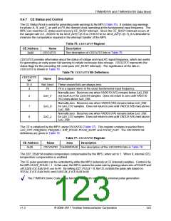
Table 75: CESTATUS Register
CE Address
Name
Description
CESTATUS
See description of CESTATUS bits in Table 76.
0x80
CESTATUS provides information about the status of voltage and input AC signal frequency, which are useful
for generating an early power fail warning to initiate necessary data storage. CESTATUS represents the
status flags for the preceding CE code pass (CE_BUSY interrupt). The significance of the bits in
CESTATUS is shown in Table 76.
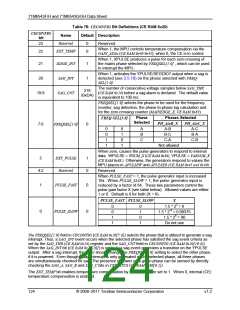
Table 76: CESTATUS Bit Definitions
CESTATUS
Name
Description
bit
31:4
3
Not Used
These unused bits are always zero.
F0
F0 is a square wave at the exact fundamental input frequency.
Normally zero. Becomes one when VADC10 (VC) remains below SAG_THR
(CE RAM 0x24) for SAGCNT samples. Does not return to zero until VADC10
(VC) rises above SAG_THR.
SAG_C
SAG_B
SAG_A
2
1
0
Normally zero. Becomes one when VADC9 (VB) remains below SAG_THR
for SAG_CNT samples. Does not return to zero until VADC9 (VB) rises above
SAG_THR.
Normally zero. Becomes one when VADC8 (VA) remains below SAG_THR
for SAG_CNT samples. Does not return to zero until VADC8 (VA) rises above
SAG_THR.
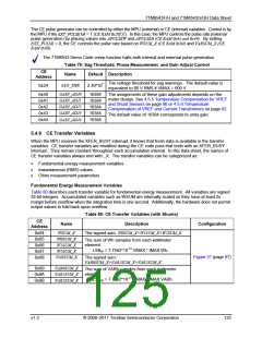
The CE is initialized by the MPU using CECONFIG (Table 77). This register contains in packed form
SAG_CNT, FREQSEL0, FREQSEL1, EXT_PULSE, PULSE_SLOW, and PULSE_FAST. The CECONFIG bit
definitions are given in Table 78.
Table 77: CECONFIG Register
CE Address
Name
Data
Description
CECONFIG
See description of the CECONFIG bits in Table 78.
0x20
0x0030DA20
The EXT_TEMP bit enables temperature compensation by the MPU, when set to 1. When 0, internal (CE)
temperature compensation is enabled.
The CE pulse generator can be controlled by either the MPU (external) or CE (internal) variables. Control is by
the MPU if EXT_PULSE = 1. In this case, the MPU controls the pulse rate by placing values into APULSEW and
APULSER (CE RAM 0x45 and 0x49). By setting EXT_PULSE = 0, the CE controls the pulse rate based on
WSUM_X (CE RAM 0x84) and VARSUM_X (CE RAM 0x88).
The 71M6543 Demo Code creep function halts both internal and external pulse generation.
v1.2
© 2008–2011 Teridian Semiconductor Corporation
123

 MAXIM [ MAXIM INTEGRATED PRODUCTS ]