71M6543F/H and 71M6543G/GH Data Sheet
the source for pulse generation in APULSEW and APULSER to generate pulses. Irrespective of the
EXT_PULSE status, the output pulse rate controlled by APULSEW and APULSER is implemented by the CE
only. By setting EXT_PULSE = 1, the MPU is providing the source for pulse generation. If EXT_PULSE is 0,
W0SUM_X and VAR0SUM_X are the default pulse generation sources. In this case, creep cannot be
controlled since it is an MPU function.
The maximum pulse rate is 3*FS = 7.5 kHz.
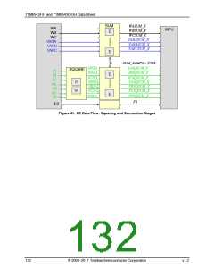
See 2.3.6.2 VPULSE and WPULSE (page 27) for details on how to adjust the timing of the output pulses.
The maximum time jitter is 1/6 of the multiplexer cycle period (nominally 67 µs) and is independent of the
number of pulses measured. Thus, if the pulse generator is monitored for one second, the peak jitter is
67 ppm. After 10 seconds, the peak jitter is 6.7 ppm. The average jitter is always zero. If it is attempted
to drive either pulse generator faster than its maximum rate, it simply outputs at its maximum rate without
exhibiting any rollover characteristics. The actual pulse rate, using WSUM as an example, is:
WRATE ⋅WSUM ⋅ FS ⋅ X
,
RATE =
Hz
246
where FS = sampling frequency (2184.53 Hz), X = Pulse speed factor derived from the CE variables
PULSE_SLOW (CE RAM 0x20[0]) and PULSE_FAST (CE RAM 0x20[1]).
Table 85: CE Pulse Generation Parameters
CE
Name
Default
Description
Address
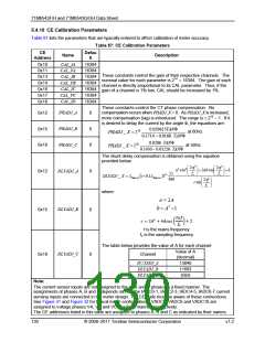
Kh = VMAX*IMAX*K / (WRATE*NACC*X) Wh/pulse
where:
K = 76.3594 when used with local sensors (CT or shunt)
K = 54.5793 when used with 71M6xx3 remote sensors
WRATE
0x21
227
KVAR
0x22
0x23
6444
2184
Scale factor for VAR measurement.
Number of samples per accumulation interval, as specified in
SUM_SAMPS[12:0], I/O RAM 0x2107[4:0], 0x2108[7:0] (NACC).
SUM_PRE
Wh pulse (WPULSE) generator input to be updated by the MPU
when using external pulse generation. The output pulse rate is:
APULSEW * FS * 2-32 * WRATE * X * 2-14.
This input is buffered and can be updated by the MPU during a
conversion interval. The change takes effect at the beginning of
the next interval.
APULSEW
0x45
0
WPULSE_CTR
0x46
0x47
0
0
Counter for WPULSE output.
Unsigned numerator, containing a fraction of a pulse. The value
in this register always counts up towards the next pulse.
WPULSE_ FRAC
WSUM_ ACCUM
APULSER
0x48
0x49
0x4A
0
0
0
Roll-over accumulator for WPULSE.
VARh (VPULSE) pulse generator input.
Counter for VPULSE output.
VPULSE_CTR
Unsigned numerator, containing a fraction of a pulse. The value
in this register always counts up towards the next pulse.
VPULSE_ FRAC
VSUM_ACCUM
0x4B
0x4C
0
0
Roll-over accumulator for VPULSE.
Other CE Parameters
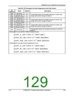
Table 86 shows the QUANT CE parameters used for suppression of noise due to scaling and truncation
effects. The equations for calculating the LSB weight of each QUANT parameter are provided at the
bottom of Table 86.
128
© 2008–2011 Teridian Semiconductor Corporation
v1.2

 MAXIM [ MAXIM INTEGRATED PRODUCTS ]