71M6543F/H and 71M6543G/GH Data Sheet
5.3
Reading the Info Page (71M6543H and 71M6543GH only)
High precision trim fuse values provided in the 71M6543H and 71M6543GH devices cannot be directly
accessed through the I/O RAM space. These trim fuses reside in a special area termed the “Info Page”.
The MPU gains access to the Info Page by setting the INFO_PG (I/O RAM 0x270B[0]) control bit. Once the
INFO_PG bit is set, Info Page contents are accessible in program memory space based at the address
specified by the contents of CE_LCTN[6/5:0] (I/O RAM 0x2109[5:0]) in the 71M6543H and CE_LCTN[6:0]
(I/O RAM 0x2109[6:0]) in the 71M6543GH. CE_LCTN[5:0] in the 71M6543H and CE_LCTN[6:0] in the
71M6543GH specify a base address at a 1KB address boundary. Thus, the base address for the Info Page
is at 1024*CE_LCTN[5:0] in the 71M6543H and 1024*CE_LCTN[6:0] in the 71M6543GH. Table 72 provides
a list of the available 71M6543H and 71M6543GH trim fuses and their corresponding offsets relative to
the Info Page base address. After reading the desired Info Page information, the MPU must reset the
INFO_PG bit.
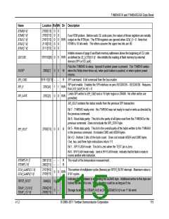
Table 72: Info Page Trim Fuses
Trim Fuse
Object Size
Address Offset
Comments
TEMP_85[10:0] holds the
STEMP[10:0] reading at 85°C.
2’s complement format
TEMP_85[10:8]
TEMP_85[7:0]
(11-bits)
8-bits
8-bits
0x90
0x91
TRIMBGB[15:0] holds the
deviation of VREF from its ideal
value (1.195V) at 85°C.
LSB = 0.1 mV
TRIMBGB[15:8]
TRIMBGB[7:0]
(16-bits)
8-bits
8-bits
0x92
0x93
2’s complement format
TRIMBGD[7:0] holds the
deviation of VREF from its ideal
value (1.195V) at 22°C.
LSB = 0.1 mV
TRIMBGD[7:0]
(8-bits)
8-bits
0x94
2’s complement format
LCDADJ12 = [VLCD-3.676v] at
22C when LCD_DAC=0C.
LSB=5mV. Two’s complement.
LCDADJ0 = [VLCD-2.65v] at
22C when LCD_DAC=0.
LCDADJ12[7:0]
(8-bits)
8-bits
8-bits
0x95
0x96
LCDADJ0[7:0]
(8-bits)
LSB=5mV. Two’s complement.
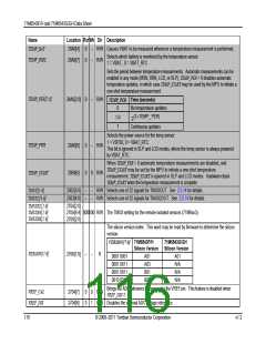
Figure 38. Trim Fuse Bit Mapping
Offset
0x90
0x91
0x92
0x93
0x94
Name
Bit 7
Bit 6
Bit 5
Bit 4 Bit 3 Bit 2 Bit 1 Bit 0
TEMP_85[10:8]
TEMP_85[10:0]
TEMP_85[7:0]
TRIMBGB[15:8]
TRIMBGB[7:0]
TRIMBGD[7:0]
TRIMBGB[15:0]
TRIMBGD[7:0]
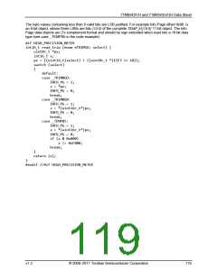
The code below provides an example for reading Info Page fuse trims. In this code example, the address,
"px" is a pointer to the MPU’s code space. In assembly language, the Info Page data objects, which are
read-only, must be accessed with the MOVC 8051 instruction.
In C, Info Page trim fuses must be fetched with a pointer of the correct width, depending whether an 8-bit
or a 16-bit data object is to be fetched. The case statements in the code example below perform casts to
obtain a pointer of the correct size for each object, as needed.
In assembly language, the MPU has to form 11-bit or 16-bit values from two separate 8-bit fetches,
depending on the object being fetched.
118
© 2008–2011 Teridian Semiconductor Corporation
v1.2

 MAXIM [ MAXIM INTEGRATED PRODUCTS ]