71M6543F/H and 71M6543G/GH Data Sheet
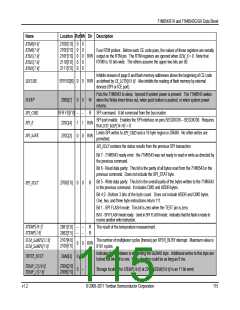
Name
Location Rst Wk Dir Description
RTM0[9:8]
RTM0[7:0]
RTM1[7:0]
RTM2[7:0]
RTM3[7:0]
210D[1:0]
210E[7:0]
210F[7:0]
2110[7:0]
2111[7:0]
0
0
0
0
0
0
0
0
0
0
Four RTM probes. Before each CE code pass, the values of these registers are serially
R/W output on the RTM pin. The RTM registers are ignored when RTM_E = 0. Note that
RTM0 is 10 bits wide. The others assume the upper two bits are 00.
Inhibits erasure of page 0 and flash memory addresses above the beginning of CE code
R/W as defined by CE_LCTN[6/5:0]. Also inhibits the reading of flash memory by external
devices (SPI or ICE port).
SECURE
SLEEP
SFR B2[6]
28B2[7]
0
0
0
0
Puts the 71M6543 to sleep. Ignored if system power is present. The 71M6543 wakes
W
when the Wake timer times out, when push button is pushed, or when system power
returns.
SPI_CMD
SPI_E
SFR FD[7:0] –
–
1
R
SPI command. 8-bit command from the bus master.
SPI port enable. Enables the SPI interface on pins SEGDIO36 – SEGDIO39. Requires
that LCD_MAP[36-39] = 0.
270C[4]
270C[3]
1
0
R/W
Limits SPI writes to SPI_CMD and a 16 byte region in DRAM. No other writes are
permitted.
SPI_SAFE
0
R/W
SPI_STAT contains the status results from the previous SPI transaction
Bit 7 - 71M6543 ready error: the 71M6543 was not ready to read or write as directed by
the previous command.
Bit 6 - Read data parity: This bit is the parity of all bytes read from the 71M6543 in the
previous command. Does not include the SPI_STAT byte.
Bit 5 - Write data parity: This bit is the overall parity of the bytes written to the 71M6543
in the previous command. It includes CMD and ADDR bytes.
SPI_STAT
2708[7:0]
0
0
R
Bit 4:2 - Bottom 3 bits of the byte count. Does not include ADDR and CMD bytes.
One, two, and three byte instructions return 111.
Bit 1 - SPI FLASH mode: This bit is zero when the TEST pin is zero.
Bit 0 - SPI FLASH mode ready: Used in SPI FLASH mode. Indicates that the flash is ready to
receive another write instruction.
STEMP[10:3]
STEMP[2:0]
2881[7:0]
2882[7:5]
–
–
–
–
R
R
The result of the temperature measurement.
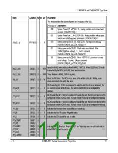
SUM_SAMPS[12:8]
SUM_SAMPS[7:0]
2107[4:0]
2108[7:0]
The number of multiplexer cycles (frames) per XFER_BUSY interrupt. Maximum value is
8191 cycles.
0
0
0
0
0
–
R/W
R
Indicates that hardware is still writing the 0x28A0 byte. Additional writes to this byte are
locked out while it is one. Write duration could be as long as 6 ms.
TBYTE_BUSY
28A0[3]
TEMP_22[10:8]
TEMP_22[7:0]
230A[2:0]
230B[7:0]
R
Storage location for STEMP[10:0] at 22C. STEMP[10:0] is an 11 bit word.
v1.2
© 2008–2011 Teridian Semiconductor Corporation
115

 MAXIM [ MAXIM INTEGRATED PRODUCTS ]