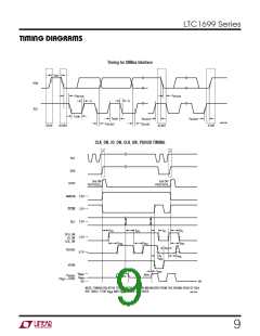
LTC1699 Series
U
W
U U
APPLICATIO S I FOR ATIO
Register 1. After issuing the final acknowledgement bit,
the SMBus interface returns to an idle state and waits for
the next start bit.
After power-up, the microprocessor must set up the
registers before the LTC1699-80, LTC1699-81 and
LTC1699-82 recognizes On protocols. This requirement
ensures that the correct DC/DC converter output is pro-
grammedbeforetheconvertersareturnedon. Aftersetup,
Read-Back allows the contents of Registers 0 and 1 to be
verified in case the VID codes were corrupted by noise or
bus conflicts.
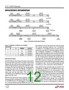
Read Word Protocol
The Read Word protocol starts off like Write Word proto-
col but after the command code acknowledgment, the
microprocessor issues a second start bit (called a re-
peatedstart).Thisisfollowedbytheslaveaddressbutwith
the R/W bit set high to indicate that data direction is now
from the LTC1699-80, LTC1699-81 or LTC1699-82 to the
microprocessor. The LTC1699-80, LTC1699-81 or
LTC1699-82 then acknowledges the slave address and
clocks the contents of Register 0 (Data Low byte) to the
microprocessor. The Data Low byte is acknowledged by
the microprocessor. On detecting the acknowledgment
bit, the LTC1699-80, LTC1699-81 or LTC1699-82 clocks
out the contents of Register 1 (Data High byte). As defined
in the SMBus specifications, the microprocessor does not
acknowledge the last data byte. The LTC1699-80,
LTC1699-81orLTC1699-82entersanidlestatetowaitfor
the next start bit after clocking out the Data High byte. The
five most significant bits (VID0-VID4) of the Data Low and
High bytes are the resistor divider settings previously
loaded using the Setup protocol. The next bit below the
VID0-VID4 bits is the status of the DCON signal. If this bit
is low (high), the DC/DC converters are switched on (off).
The two unused, least significant bits of the Data Low and
Data High bytes are clocked out as zeros which removes
the need to mask out these bits in software.
In order to turn on the DC/DC converter, two On protocols
mustbesenttoslaveaddressE2Hwithoutanyother(E2H)
protocols in between. Protocols to other slave addresses
are still allowed and are ignored. Similarly, two Off proto-
cols must be sent to slave address E2H to turn the
converters off. The On and Off protocols are monitored by
aninternalstatemachine. Theoutputofthestatemachine,
SMBON, is high after two On commands and low after two
Off commands. Repeated On and Off protocols reduce the
chances of bus conflicts and noise turning the converter
on or off accidentally. In both On and Off protocols, the
LTC1699-80, LTC1699-81 and LTC1699-82, do not latch
in the Data Low and Data High bytes. This protects the
settings that have already been loaded into the registers
and verified by read-back.
Once the converters are turned on (both SMBON and
VRON are high) the contents of Registers 0 and 1 are
protected and can only be altered with Setup protocols if
VRON is pulled low or two Off protocols are sent to the
LTC1699-80,LTC1699-81orLTC1699-82(toforceSMBON
low).
DC/DC Converter Control
Safeguards
The LTC1699-80, LTC1699-81 and LTC1699-82 provide
sixpinsforDC/DCconvertercontrol:SEL,VRON,CPU_ON,
IO_ON,CLK_ONandPGOOD.Thesepins(exceptSEL)and
the output of the internal on/off state machine (SMBON)
determine if the DC/DC converters are operating or in
shutdown.
The LTC1699-80, LTC1699-81 and LTC1699-82 provide
safeguards against incorrect divider codes and the unin-
tentional turn-on or turn-off of the DC/DC converters.
Incorrect codes due to bus conflicts during Setup proto-
cols can cause damage to circuits powered by the DC/DC
converters. The safeguards built into the LTC1699-80,
LTC1699-81 and LTC1699-82 include Read-Back, re-
peated On and Off protocols, ignoring On protocols if the
registers have not been setup, locking out registers while
the DC/DC converters are operating and latching in VID
codes only in Setup protocols.
The SEL and VRON pins are TTL compatible, high imped-
ance inputs with a logic threshold of 1.3V over the entire
2.7V to 5.5V supply range. They are compatible with 3.3V
logic and have ±50mV of hysterisis for noise rejection.
When pulled high or low, the SEL pin selects Register 1
and 0 respectively as the active divider setting. The VRON
13

 Linear [ Linear ]