LTC1699 Series
U
W
U U
APPLICATIO S I FOR ATIO
output voltage of a DC/DC converter that generates the
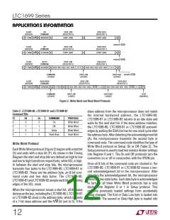
CPU core supply voltage. Its programmable ratios (see
Table1)aredesignedfor0.8V-referencedconverterssuch
as the LTC1628, LTC1702, LTC1735 and LTC1778 and
comply with the Intel 5-bit desktop (VRM8.4 for
LTC1699-81 and VRM9.0 for LTC1699-82) and 5-bit
mobile VID codes. On power-up, the outputs of both
registers are internally set to 11111B.
DC converter respectively. The output of the DC/DC con-
verter is given by:
V
OUT = VREF • (RFB2+RFB1)/RFB2
where VREF is the internal reference voltage of the con-
verter. Each resistor has a tolerance of ±30% but the ratio,
(RFB2+RFB1)/RFB2, is specified to within ±0.35% over
temperature. The error budget for the DC/DC converter
output voltage must include the ±0.35% ratio tolerance
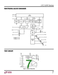
The LTC1699-80, LTC1699-81 and LTC1699-82 provide
three pins, CPU_ON, IO_ON, and CLK_ON to (optionally)
control three DC/DC converters that generate the CPU, I/O
and clock buffer VCC voltages in a VRM. These open drain,
N-channeloutputpinsusuallyconnecttotheRUN/SSpins
of the converters and pull low to shut down the converters
or become a high impedance state to allow the converters
to soft-start.
and the tolerance in VREF
.
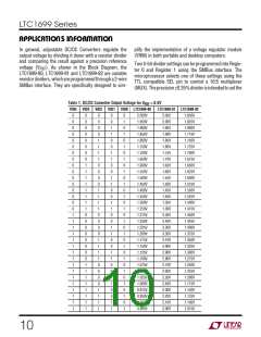
The value of RFB1 is fixed and RFB2 is changed to vary the
divider setting. The value of RFB2 for any divider setting
can be calculated from the above equation, assuming that
RFB1 = 10kΩ for the LTC1699-80 and LTC1699-82 and
20kΩ for the LTC1699-81. Table 1 shows the output
voltage of a DC/DC converter (VREF = 0.8V) for all 32
settings of the resistor divider. The divider setting is
determined by the outputs (VID0-VID4) of the register
selected by the SEL pin.
The PGOOD pin is driven from an internal timer that pulls
PGOOD low for 50µs typical whenever the resistor divider
setting is changed or the converters are allowed to soft-
start. Over the entire temperature and supply voltage
range, the timer low period is 70µs max which meets the
100µs max converter output settling time specified by
Intel. The PGOOD pin, if tied to the FCB pin of an LTC DC/
DC converter, reduces the time needed for the converter
output to decrease to a lower voltage under light load
conditions by forcing the converter into continuous mode
for 50µs.
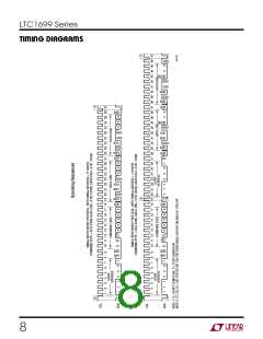
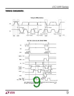
SMBus Interface
The SMBus interface uses two wires: SDA and SCL. Data
totheLTC1699-80,LTC1699-81orLTC1699-82,islatched
at the rising edge of the SCL clock input and shifted out at
the falling edge. The VIL and VIH logic threshold voltages
of the SDA and SCL pins are 0.8V and 2.1V respectively
and comply with Rev 1.1 version of the Intel System
Management Bus Specifications.
The TTL compatible VRON input pin and the output of the
internalon/offstatemachine(SMBON)controlthestateof
the CPU_ON, IO_ON, CLK_ON and PGOOD pins. SMBON
is accessed using SMBus protocols and must be pro-
grammedtoahighstatebeforetheconverterscanturnon.
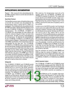
The SMBus protocols (see Figure 2) incorporate safe-
guards against errors caused by bus conflicts.
TheWriteWordandReadWordprotocols(Figure2)share
three common features. First, the 7-bit slave address for
bothprotocolsisinternallyhardwiredto1110001B=E2H.
A single R/W bit follows the slave address. This bit is low
fordatatransferfromthemicroprocessortotheLTC1699-
80, LTC1699-81 or LTC1699-82 and high for transfers in
the opposite direction.
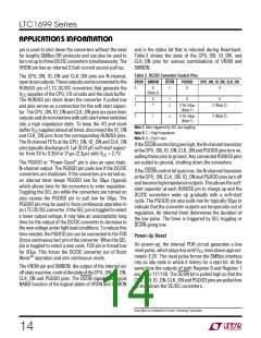
Resistor Divider
Second, the LTC1699-80, LTC1699-81 and LTC1699-82
decode only the three most significant bits of the 8-bit
command code. Table 2 shows the four valid combina-
tions. All other combinations are ignored.
The resistor divider is designed specifically for DC/DC
converters, such as the LTC1628, LTC1702, LTC1735,
LTC1778 and LTC1929 with a reference voltage of 0.8V. It
consists of a fixed resistor, RFB1 connected between the
SENSE and FB pins and a variable resistor, RFB2, con-
nected between the FB and GND pins. The SENSE and FB
pins are tied to the output and feedback nodes of the DC/
Third, the Data Low and Data High bytes correspond to
Registers 0 and 1 respectively. In Write Word protocol with
C7 = C6 = 0, C5 = 1, the five most significant bits (VID0-
VID4) of these bytes specify a resistor divider setting.
11

 Linear [ Linear ]