LTC1699 Series
U
W
U U
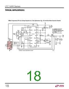
APPLICATIO S I FOR ATIO
pin is used to shut down the converters without the need
for lengthy SMBus Off protocols and can also be used to
turn on up to three DC/DC converters simultaneously. The
VRON pin has an internal 2.5uA current source pull-up.
and is the status bit that is returned during Read-back.
Table 3 shows the state of the CPU_ON, IO_ON, and
CLK_ON pins for various combinations of VRON and
SMBON.
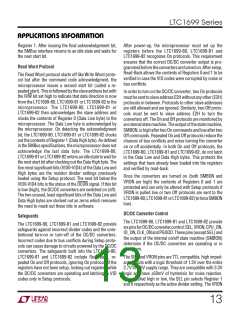
Table 3. DC/DC Converter Control Pins
The CPU_ON, IO_ON and CLK_ON pins are N-channel,
opendrainoutputs.Theseoutputscanbeconnectedtothe
RUN/SS pin of LTC DC/DC converters that generate the
VRON SMBON
DCON
PGOOD
CPU_ON, IO_ON, CLK_ON
0
X
1
0
0
(Note 3)
V
CC supplies of the CPU, I/O circuits and the clock buffer.
1
1
0
1
0
0
The RUN/SS pin shuts down the converter if pulled low
and also serves as a connection for the soft-start capaci-
tor. The CPU_ON, IO_ON and CLK_ON pins are open drain
outputs and do not interfere with soft-start when switched
into a high impedance state. To keep the I/O and clock
bufferVCC suppliesaliveatalltimes,disconnecttheIO_ON
and CLK_ON pins from the corresponding RUN/SS pins.
The N-channel FETs at the CPU_ON, IO_ON and CLK_ON
pinstypicallydischargea0.1µF(0.01µF)soft-startcapaci-
tor from 3V to 0.35V in 21µs (2.3µs) with VCC = 2.7V.
↑
↓
0 for 50µs
(Note 1)
Z (Note 2)
↑
1
↓
0 for 50µs
Z (Note 2)
(Note 1)
Note 1: Also triggered by SEL pin toggling.
Note 2: Z = High Impedance
Note 3: X = Don’t care
IftheDCONcontrolbitgoeshigh, theN-channeltransistor
attheCPU_ON, IO_ON, CLK_ONandPGOODpinsturnon,
pulling these pins to ground. Any connected RUN/SS pins
are pulled to ground, shutting down the converters.
The PGOOD or “Power Good” pin is also an open drain,
N-channel output. The PGOOD pin pulls low if the DC/DC
converters are shutdown. If the converters are turned on,
an internal timer keeps PGOOD low for 50µs (typical)
which allows time for the converters to enter regulation.
Toggling the SEL pin while the converters are turned on
also causes the PGOOD pin to pull low for 50µs. The
PGOOD pin may be used to force continuous operation in
an LTC DC/DC converter. If the SEL pin is toggled to select
a lower output voltage, it may take an unacceptably long
time for the output of the DC/DC converter to decrease to
thenewvoltageunderlightloadconditions. Toreducethis
time needed, the PGOOD pin can be connected to the FCB
(force continuous bar) pin of the converter. When the SEL
pin is toggled to select a new code, FCB pin is forced low
for 50µs. This forces the DC/DC converter out of Burst
ModeTM operation and into continuous mode.
If the DCON control bit goes low, the N-channel transistor
at the CPU_ON, CLK_ON, IO_ON and PGOOD pins turn off
andbecomehighimpedanceoutputs.Thisallowsthesoft-
start capacitor at each RUN/SS pin to charge up and the
DC/DC converters wake up gradually with a soft-start
cycle. The PGOOD pin also pulls low for typically 50µs to
indicate that the converter outputs are temporarily out of
regulation. An internal timer determines the duration of
the low pulse. The timer is triggered by SEL toggling or
DCON going low.
Power-Up Reset
On power-up, the internal POR circuit generates a low
reset pulse, which stays low until VCC rises above approxi-
mately 2.2V. The reset pulse forces the SMBus interface
into an idle state in which it listens for a start bit. At the
same time the outputs of both Register 0 and Register 1
are set to 11111B. The DCON bit is pulled high so that the
CPU_ON, IO_ON, CLK_ONandPGOODpinsarepulledlow
to shut down the DC/DC converters.
The VRON pin and SMBON, the output of the internal on/
offstatemachine,controlthestateoftheCPU_ON,IO_ON,
CLK_ON and PGOOD pins. The DCON signal is a logical
NAND function of the logical states of VRON and SMBON
Burst Mode is a trademark of Linear Technology Corporation.
14

 Linear [ Linear ]