LTC1699 Series
U
W
U U
APPLICATIO S I FOR ATIO
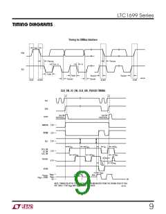
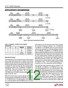
SLAVE
ON
DATA LOW
(REGISTER 0)
DATA HIGH
(REGISTER 1)
ADDRESS
COMMAND
S 1110001 R/W A 000XXXXX
A
A
A
DON’T CARE
A
DON’T CARE
A P
UPDATE DCON
SLAVE
ADDRESS
OFF
COMMAND
DATA LOW
(REGISTER 0)
DATA HIGH
(REGISTER 1)
S 1110001 R/W A 011XXXXX
DON’T CARE
A
DON’T CARE
A P
UPDATE DCON
SLAVE
ADDRESS
SETUP
COMMAND
DATA LOW
(REGISTER 0)
DATA HIGH
(REGISTER 1)
S 1110001 R/W A 001XXXXX
VID4 VID3 VID2 VID1 VID0 X X X
A
VID4 VID3 VID2 VID1 VID0 X X X
A P
COMMAND
LATCHED
DATA LOW
LATCHED
DATA HIGH UPDATE DCON
LATCHED
SLAVE
ADDRESS
READ-BACK
COMMAND
DATA LOW
(REGISTER 0)
DATA HIGH
(REGISTER 1)
S 1110001 R/W A 010XXXXX
A
S 1110010 RD
A
VID4 VID3 VID2 VID1 VID0 DCON 0 0
A
VID4 VID3 VID2 VID1 VID0 DCON 0 0 A P
COMMAND
LATCHED
DATA LOW
LOADED
DATA HIGH
LOADED
STOP
(IGNORED)
Figure 2. Write Word and Read Word Protocols
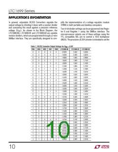
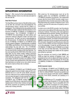
Table 2. LTC1699-80, LTC1699-81 and LTC1699-82
Command Bits
slave address from the microprocessor does not match
the internal hardwired address, the LTC1699-80,
LTC1699-81 or LTC1699-82 returns to an idle state and
waits for the next start bit. If the slave address matches,
the LTC1699-80, LTC1699-81 or LTC1699-82 acknowl-
edges by pulling the SDA line low for one clock cycle after
theaddressbyte. Afterdetectingtheacknowledgementbit
(A), the microprocessor transmits the second byte or
command code. The command code identifies the type of
Write Word protocol as Setup, On or Off (Table 2). The
Setupprotocolisusedtoloadtworesistordividersettings
into Register 0 and 1. The On and Off protocols turn the
converters on or off in conjunction with the VRON pin.
C7
0
C6
0
C5
0
COMMAND
On
PROTOCOL
Write Word
Write Word
Write Word
Read Word
0
1
1
Off
0
0
1
Setup
0
1
0
Read-Back
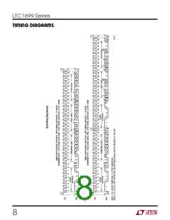
Write Word Protocol
Each Write Word protocol (Figure 2) begins with a start bit
(S) and ends with a stop bit (P). As shown in the Timing
Diagram the start and stop bits are defined as high to low
and low to high transitions respectively, while SCL is high.
In between the start and stop bits, the microprocessor
transmits four bytes to the LTC1699-80, LTC1699-81 or
LTC1699-82. These are the address byte, an 8-bit com-
mand code and two data bytes. The LTC1699-80,
LTC1699-81andLTC1699-82sampleeachbitattherising
edges of the SCL clock.
Once all 8 bits of the command code are clocked in, the
LTC1699-80, LTC1699-81 or LTC1699-82 issues a sec-
ond acknowledgement bit to the microprocessor. After
detecting the acknowledgement bit, the microprocessor
transmits two data bytes. Each data byte is acknowledged
in turn for all three Write Word protocols but is only
latched into Register 0 or 1 in Setup protocol. This
prevents previously loaded settings from accidentally
being changed. The first or Data Low byte is loaded into
Register 0. The second or Data High byte is loaded into
When the microprocessor issues a start bit, all the slave
devicesonthebus,includingtheLTC1699-80,LTC1699-81
or LTC1699-82 clock in the address byte, which consists
of a 7-bit slave address and the R/W bit (set to 0). If the
12

 Linear [ Linear ]