LTC5588-1
APPLICATIONS INFORMATION
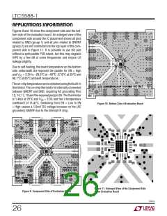
Evaluation Board
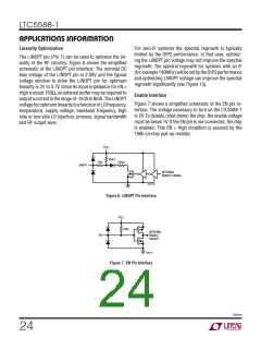
voltage drop over R1 and R2 is about 0.15V. The supply
voltages applied directly to the chip can be monitored
by measuring at the test points TP1 and TP2. If a power
supply is used that ramps up slower than 7V/μs and limits
the overshoot on the supply below 3.8V, R1 and R2 can be
omitted. To facilitate turn-on and turn-off time measure-
ments, the microstrip between J5 and J7 can be used
connecting J5 to a pulse generator, J7 to an oscilloscope
with 50Ω input impedance, removing R5 and inserting a
0Ω resistor for R3.
Figure 8 shows the evaluation board schematic. A good
ground connection is required for the exposed pad. If this
is not done properly, the RF performance will degrade.
Additionally, theexposedpadprovidesheatsinkingforthe
part and minimizes the possibility of the chip overheat-
ing. Resistors R1 and R2 reduce the charging current in
capacitors C1 and C2 (see Figure 8) and will reduce supply
ringing during a fast power supply ramp-up with induc-
tive wiring connecting V and GND. For EN = High, the
CC
J9
BBMI
J8
BBPI
R6
OPT
C12
C11
R11
OPT
R10
OPT
OPT
OPT
J7
EN
R4
OPT
TP1
EN
V
CC
C1
4.7μF
C3
1nF
R1
J5
1Ω
R2
1.3Ω
EN
R5
0Ω
R3
OPT
TP2
C4
1nF
C2
4.7μF
24 23 22 21 20 19
C5
J1
LOP
1nF
1
18
17
16
15
14
13
EN
V
CC2
C7
6.8pF
J6
RF OUT
2
3
4
5
6
6
5
4
GND
LOP
LOM
GND
NC
GNDRF
RF
NC GND BP
BALUN
U2
OPT
U1
LTC5588-1
C8
0.2pF
UNBP GND BP
NC
1
2
3
GNDRF
NC
C14
1nF
J2
LOM
R12
OPT
C6
1nF
LINOPT
R14
1Ω
25
7
8
9
10 11 12
26
BOARD NUMBER: DC1524A
GND
C13
100nF
R13
OPT
J3
BBMQ
J4
BBPQ
C9
OPT
C10
OPT
R8
OPT
R9
OPT
R7
OPT
55881 F08
Figure 8. Evaluation Circuit Schematic
55881fb
25

 Linear [ Linear ]