LTC5588-1
APPLICATIONS INFORMATION
Table 5. LOM Port Input Impedance vs Frequency for EN = Low
and PLOM = 10dBm (LOP Terminated with 50Ω AC to Ground)
0
–2
REFLECTION COEFFICIENT
FREQUENCY
(GHz)
LOM INPUT
IMPEDANCE
MAG
0.48
ANGLE
–32.1
–36.9
–42
–4
0.2
0.25
0.3
0.4
0.5
0.6
0.7
0.8
0.9
1.0
1.2
1.4
1.6
1.8
2.0
2.5
3.0
3.5
4.0
4.5
5.0
5.5
6.0
92-j61
83-j55
75-j50
66-j39
60-j32
56-j27
53-j23
50-j20
48-j19
46-j17
42-j15
40-j14
38-j14
37-j13
36-j12
35-j7.5
31-j2.2
27+j1.3
24+j2.7
22+j4.4
20+j6.8
18+j8.5
16+j9.5
0.444
0.414
0.345
0.293
0.251
0.225
0.199
0.191
0.18
–6
3.3V, 85°C
3.3V, 25°C
3.15V, 25°C
3.45V, 25°C
3.3V, –40°C
–49.3
–57.4
–63.2
–71.2
–78.8
–86.6
–93.6
–108
–117
–123
–127
–132
–150
–172
175
–8
–10
300
400
500
600
RF FREQUENCY (MHz)
200
55881 F05
Figure 5. Low Band Voltage Gain vs RF Frequency
Using Figure 4 Matching
0.181
0.192
0.205
0.211
0.212
0.202
0.244
0.31
The third harmonic content of the LO can degrade image
rejectionseverely,itisrecommendedtokeepthe3rd-order
harmonic of the LO signal lower than the desirable image
rejectionminus6dB.Althoughthesecondharmoniccontent
of the LO is less sensitive, it can still be significant. The
large-signal noise figure can be improved with higher LO
input power. However, if the LO input power is too large to
cause the internal LO signal clipping in the phase-shifter
section, the image rejection can be degraded rapidly.
This clipping point depends on the supply voltage, LO
frequency,temperatureandsingleendedvsdifferentialLO
drive. At f = 2140MHz, V = 3.3V, T = 25°C and single-
0.363
0.389
0.433
0.479
0.525
171
166
160
157
154
LO
CC
ended LO drive, this clipping point is at about 16.7dBm.
For 3.15V it lowers to 16.1dBm. For differential drive it is
about 21.6dBm.
0
–10
–20
–30
RF PORT, EN = HIGH,
C7 = 4.7nH, C8 = 33pF
RF PORT, EN = LOW,
C7 = 4.7nH, C8 = 33pF
RF PORT, EN = HIGH,
C7 = 2.7nH, C8 = 10pF
RF PORT, EN = LOW,
C7 = 2.7nH, C8 = 10pF
LO PORT, EN = HIGH,
USING B0310J50100A00
LO PORT, EN = LOW,
USING B0310J50100A00
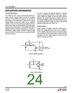
The differential LO port input impedance for EN = High
and P = 10dBm is given in Table 6.
LO
–40
200
400
500
600
300
FREQUENCY (MHz)
55881 F04
Figure 4. RF and LO Port Return Loss vs Frequency for Low Band
Match (See Figure 8)
55881fb
21

 Linear [ Linear ]