LTC5588-1
APPLICATIONS INFORMATION
Linearity Optimization
For zero-IF systems the spectral regrowth is typically
limited by the OIP2 performance. In that case, optimiz-
ing the LINOPT pin voltage may not improve the spectral
regrowth. The spectral regrowth for systems with an IF
(forexample140MHz)willbesetbytheOIP3performance
and optimizing LINOPT voltage can improve the spectral
regrowth significantly (see Figure 13).
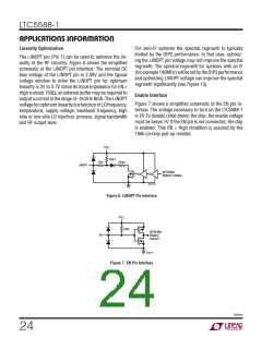
The LINOPT pin (Pin 7) can be used to optimize the lin-
earity of the RF circuitry. Figure 6 shows the simplified
schematic of the LINOPT pin interface. The nominal DC
bias voltage of the LINOPT pin is 2.56V and the typical
voltage window to drive the LINOPT pin for optimum
linearity is 2V to 3.7V. Since its input impedance for EN =
High is about 150Ω, an external buffer may be required to
output a current in the range of –2mA to 8mA. The LINOPT
voltageforoptimumlinearityisafunctionofLOfrequency,
temperature, supply voltage, baseband frequency, high
side or low side LO injection, process, signal bandwidth
and RF output level.
Enable Interface
Figure 7 shows a simplified schematic of the EN pin in-
terface. The voltage necessary to turn on the LTC5588-1
is 2V. To disable (shut down) the chip, the enable voltage
must be below 1V. If the EN pin is not connected, the chip
is enabled. This EN = High condition is assured by the
100k on-chip pull-up resistor.
V
CC1
100Ω
75Ω
250Ω
LINOPT
INTERNAL
ENABLE SIGNAL
55881 F06
Figure 6. LINOPT Pin Interface
V
CC1
100k
INTERNAL
ENABLE
CIRCUIT
EN
55881 F07
Figure 7. EN Pin Interface
55881fb
24

 Linear [ Linear ]