LTC5588-1
APPLICATIONS INFORMATION
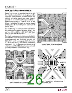
Figures 9 and 10 show the component side and the bot-
tom side of the evaluation board. An enlarged view of the
component side around the IC placement shows all pins
related to GND (group 1) and all pins related to GNDRF
(group 2) are not connected via the top layer of the com-
ponent side in Figure 11. It is possible to use the part
without a split-paddle PCB island, but this may degrade
OIP2 by a few dB at some frequencies and reduce LO
leakage slightly.
Due to self heating, the board temperature on the bottom
side underneath the exposed die paddle for EN = high
and V = 3.3V is –29.5°C at –40°C, 37.8°C at 25°C and
CC
98.1°C at 85°C ambient temperatures.
Theon-chiptemperaturecanbeobtainedusingthebuilt-in
thermistor. The on-chip thermistor is internally connected
between GNDRF and GND, requiring AC grounding Pins
12, 14, 17, 19 and the exposed pad pin 26. The thermistor
is 1.4kΩ at 25°C and V = 3.3V, and has a temperature
CC
coefficient of 11Ω/°C. Switching from EN = Low to EN
= High causes a 1.5mV DC voltage increase on the (AC
grounded) GNDRF due to the internal IR drop.
Figure 10. Bottom Side of Evaluation Board
Figure 11. Enlarged View of the Component Side
of the Evaluation Board
Figure 9. Component Side of Evaluation Board
55881fb
26

 Linear [ Linear ]