LTC5588-1
APPLICATIONS INFORMATION
At each baseband pin, a 0.146V to 0.854V swing is de-
veloped corresponding to a DAC output current of 0mA
to 20mA. A 3dB lower gain can be achieved using R1A =
R1B = 49.9Ω; R2A = R2B = Open; R2C = 100Ω; R3A =
R3B = 51Ω; L1A = L1B = L2A = L2B = 180nH; C1A = C1B
= C3A = C3B = 68pF; C2 = 56pF.
ferential LO drive (using BD1631J50100A00) with a LO
power below 10dBm. The balun (U2) can be installed
by removing C5 and C6 (see Figure 8). Using Anaren
P/N B0310J50100A00 improves image, LO leakage and
large-signal noise performance at 240MHz and 450MHz.
For this particular balun, an external blocking capacitor
is required.
LO Section
Figure 4 shows the return loss vs RF frequency for the
240MHz and 450MHz frequency bands. Figure 5 shows
the corresponding gain vs RF frequency where the gain
curve peaks at a higher frequency compared to the fre-
quency with best match. Note that the overall bandwidth
degrades tuning the matching frequency lower. A similar
technique can be used for 700MHz and 900MHz if gain
flatness is important.
The internal LO chain consists of a quadrature phase
shifter followed by LO buffers. The LOM input can be
driven single ended with 50Ω input impedance, while the
LOP input should be terminated with 50Ω through a DC
blocking capacitor.
The LOP and LOM inputs can also be driven differentially
when an exceptionally low large-signal output noise floor
is required.
Table 2. LOM Port Input Impedance vs Frequency for EN = High
and PLOM = 0dBm (LOP Terminated with 50Ω AC to Ground)
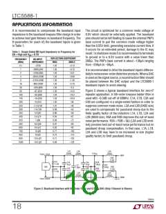
A simplified circuit schematic for the LOP and LOM inputs
is given in Figure 3. Table 2 lists LOM port input imped-
REFLECTION COEFFICIENT
FREQUENCY
(GHz)
LOM INPUT
IMPEDANCE
MAG
0.499
0.462
0.421
0.354
0.296
0.256
0.225
0.203
0.188
0.18
ANGLE
–29.8
–34.3
–38.8
–45.8
–52.4
–58.4
–64.9
–72.5
–79.6
–86.9
–101
–111
–118
–123
–128
–146
–171
176
ance vs frequency at EN = High and P
= 0dBm. For EN
LOM
0.2
0.25
0.3
0.4
0.5
0.6
0.7
0.8
0.9
1.0
1.2
1.4
1.6
1.8
2.0
2.5
3.0
3.5
4.0
4.5
5.0
5.5
6.0
98-j65
87-j58
79-j51
69-j40
63-j32
59-j27
55-j24
52-j21
50-j19
48-j18
44-j16
41-j15
39-j14
38-j13
37-j12
36-j7.8
32-j2.4
28+j1.0
25+j2.4
23+j4.1
21+j6.2
19+j7.9
17+j8.7
= Low and P
= 0dBm the input impedance is given in
LOM
Table 3. The LOM port input impedance is shown for EN
= High and Low at P = 10dBm in Table 4 and Table 5,
LOM
respectively. The circuit schematic of the demo board is
shown in Figure 8. A 50Ω termination can be connected
to the LOP port (J1).
The LOM port (J2) can also be terminated with a 50Ω
while the LO power is applied to the LOP (J1) port. In that
case, the image rejection may be degraded. At 2.14GHz,
the large-signal noise figure is about 2dB better for dif-
0.178
0.185
0.194
0.2
V
CC1
0.199
0.189
0.225
0.288
0.35
LOP
LOM
2.35V
+
(3.3V IN
–
SHUTDOWN)
173
55881 F03
0.372
0.417
0.472
0.519
168
162
Figure 3: Simplified Circuit Schematic
for the LOP and LOM inputs
159
157
55881fb
19

 Linear [ Linear ]