LTC5588-1
APPLICATIONS INFORMATION
The LTC5588-1 consists of I and Q input differential volt-
age-to-current converters, I and Q upconverting mixers,
an RF output balun, an LO quadrature phase generator
and LO buffers.
recommended. Note that the frequency of the best match
issetlowerthanthebandcenterfrequencytocompensate
the gain roll-off of the on-chip RF output balun at lower
frequency. At 240MHz and 450MHz operations, the image
rejection and the large-signal noise performance is better
using higher LO drive levels. However, if the drive level
causes internal clipping, the LO leakage degrades. Using
a balun such as Anaren P/N B0310J50100A00 increases
the LO drive level without internal clipping and provides
a relatively broadband LO port impedance match.
External I and Q baseband signals are applied to the dif-
ferential baseband input pins, BBPI, BBMI and BBPQ,
BBMQ.Thesevoltagesignalsareconvertedtocurrentsand
translated to RF frequency by means of double-balanced
upconverting mixers. The mixer outputs are combined at
the inputs of the RF output balun, which also transforms
the output impedance to 50Ω. The center frequency of
the resulting RF signal is equal to the LO signal frequency.
The LO input drives a phase shifter which splits the LO
signal into in-phase and quadrature signals. These LO
signals are then applied to on-chip buffers which drive the
upconverting mixers. In most applications, the LOM input
is driven by the LO source via a 1nF coupling capacitor,
while the LOP input is terminated with 50Ω to RF ground
via a 1nF coupling capacitor. The RF output is single ended
and internally 50Ω matched across a wide RF frequency
range from 700MHz to 5GHz with better than 10dB return
loss using C7 = 6.8pF and C8 = 0.2pF (S22 < –10dB). See
Figure 8.
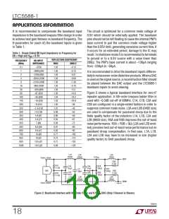
Baseband Interface
The baseband inputs (BBPI, BBMI, BBPQ, BBMQ) present
a single-ended input impedance of about –3kΩ. Because
ofthenegativeinputimpedance, itisimportanttokeepthe
sourceresistanceateachbasebandinputlowenoughsuch
that the total input impedance remains positive across the
basebandfrequency. Eachofthefourbasebandinputshas
a capacitor of 4pF in series with 14Ω connected to ground
and a PNP emitter follower in parallel (see Figure 1). The
basebandbandwidthdependsonthesourceimpedance.For
a 25Ω source impedance (50Ω terminated with 50Ω), the
baseband bandwidth (–1dB) is about 430MHz. If a 2.7nH
series inductor is inserted at each of the four baseband
inputs, the –1dB baseband bandwidth can be increased
to about 650MHz.
For 240MHz operation, C7 = 4.7nH and C8 = 33pF is rec-
ommended. For 450MHz, C7 = 2.7nH and C8 = 10pF is
LTC5588-1
RF
V
V
= 3.3V
= 3.3V
CC2
BALUN
CC1
FROM
Q CHANNEL
LOMI
LOPI
GNDRF
BBPI
14Ω
4pF
V
= 0.5V
CM
4pF
14Ω
BBMI
55881 F01
GND
Figure 1. Simplified Circuit Schematic of the LTC5588-1 (Only I Channel is Shown)
55881fb
17

 Linear [ Linear ]