LTC5588-1
APPLICATIONS INFORMATION
It is recommended to compensate the baseband input
impedance in the baseband lowpass filter design in order
to achieve best gain flatness vs baseband frequency. The
S-parameters for (each of) the baseband inputs is given
in Table 1.
The circuit is optimized for a common mode voltage of
0.5V which should be externally applied. The baseband
pins should not be left floating to cause the internal PNP’s
base current to pull the common mode voltage higher
than the 0.55V limit, generating excessive current flow. If
it occurs for an extended period, damage to the IC may
result. In shutdown mode it is recommended to terminate
to ground or to a 0.5V source with a value lower than
200Ω. The PNP’s base current is about –136μA ranging
from –250μA to –50μA.
Table 1. Single-Ended BB Input Impedance vs Frequency for
EN = High and VDC = 0.5V
REFLECTION COEFFICIENT
FREQUENCY
(MHz)
BB INPUT
IMPEDANCE
MAG
1.03
1.03
1.03
1.03
1.03
1.03
1.03
1.03
1.04
1.03
1.02
1.01
0.99
0.96
0.94
0.90
0.87
0.82
0.77
0.74
0.71
0.69
ANGLE
–0.13
–0.13
–0.37
–0.68
–1.38
–2.79
–5.3
0.1
1
–3700
–3900-j340
–3700-j950
–3200-j1500
–2100-j1900
–860-j1600
–300-j990
–87-j520
–35-j308
–16-j226
–6-j154
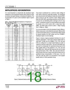
It is recommended to drive the baseband inputs differen-
tiallytoreduceeven-orderdistortionproducts.WhenaDAC
is used as the signal source, a reconstruction filter should
be placed between the DAC output and the LTC5588-1
baseband inputs to avoid aliasing.
2
4
8
16
30
Figure 2 shows a typical baseband interface for zero-IF
repeater application. A 5th-order lowpass ladder filter is
used with –0.3dB cut-off of 60MHz. C1A, C1B, C3A and
C3B are configured in a single-ended fashion in order to
suppress common mode noise. L3A and L3B (0402 size)
are used to compensate for passband droop due to the
finite quality factor of the inductors L1A, L1B, L2A and
L2B (0603 size). R3A and R3B improves the out-of-band
noise performance. R3A = R3B = 0Ω (L3A and L3B omit-
ted) provides best out-of-band noise performance but no
passband droop compensation. In that case, L1A, L1B,
L2A and L2B may have to be increased in size (higher
quality factor) to limit passband droop.
60
–10.6
–18.2
–24.8
–36
100
140
200
250
300
350
400
450
500
600
700
800
900
1000
–1.4-j120
1.4-j102
4.4-j87
–45
–52
–59
5.4-j74
–67
7-j66
–73
8.3-j58
–80
9.4-j47
–92
10-j38
–102
–113
–122
–129
10-j32
10.5-j27
10.5-j23
L1A
250nH
L2A
250nH
L3A
100nH
0.5V
DC
10mA 10mA
BBPI
R3A
71.57
R1A
R2A
C1A
C3A
71.57
1657
47pF
47pF
R2C
2497
C2
DAC
R3B
71.57
39pF
C1B
47pF
L1B
250nH
C3B
47pF
R2B
1657
R1B
71.57
L2B
250nH
L3B
100nH
BBMI
10mA 10mA
55881 F02
0.5V
DC
GND
Figure 2: Baseband Interface with 5th-Order Filter and 0.5VCM DAC (Only I Channel is Shown)
55881fb
18

 Linear [ Linear ]